Continue to Site

Welcome to EDAboard.com

Welcome to our site! EDAboard.com is an international Electronics Discussion Forum focused on EDA software, circuits, schematics, books, theory, papers, asic, pld, 8051, DSP, Network, RF, Analog Design, PCB, Service Manuals... and a whole lot more! To participate you need to register. Registration is free. Click here to register now.

ft of a transistor - non existent in the documentation.

Status
Not open for further replies.

AMSA84

Advanced Member level 2
Joined
Aug 24, 2010
Messages
577
Helped
8
Reputation
16
Reaction score
8
Trophy points
1,298
Location
Iberian Peninsula
Activity points
6,178
Hi guys,

In the documentation that I have in my possession there is no information about the ft of the transistors. Is there any way to estimate the ft of each transistors in my process? Through simulation for example.

Regards.
 

Hello,

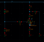
I used for such measurement next schematic:
ft_measurement.PNG

Don't look at these wires on the bulk, I just checked different transistors.

Next, I run two analysis dc and ac.
After what just use two equation:
Code:
pv("N0" "fug" ?result "dcOpInfo")
cross(dB20((mag(i("/V6/PLUS" ?result "ac")) / mag(i("/V5/PLUS" ?result "ac")))) 0 1 "either" nil nil)

for dc point for your technologe could be another parameter name, just look at available results from dc point analysis and insert it into calc.
Also, I beleive there is cadence article about right way of measurement of ft, which available on the web.
 

Hi sarge, thanks.

What about the value of lin in the current source up left? Can be any value I want? I tried different values and I got some results. However the same does not applies for the cross function. I get a value saying that returned nil. Do you know why?

EDIT: Ok, now I got some results. Are they supposed to give almost the same value? Can you explain what you did with those expressions? The first one I get it but the second I don't understand.
Regards.
 
Last edited:

HI Jairaj,

I've not read yet the article, but just by the looks it seems to be a very good article!

Thank you very much!
 

Can you explain what you did with those expressions? The first one I get it but the second I don't understand.

The second one looking where the current gain ( dB20((mag(i("/V6/PLUS" ?result "ac")) / mag(i("/V5/PLUS" ?result "ac"))) ) crosses 0 dB, this point is your ft.
 

Thanks.

And what if I want to measure the fmax?

Regards
Thanks.

And btw, why we are not biasing the gate?

Reagrds

- - - Updated - - -


Hi Jairaj

I read the link and basically it's useless because it doesn't tell how to siulate and configure cadence.

I don't understand why people do this kind of useless article in which they say how to simulate in this case the fmax and then they talk about everything and they don't say actually how to simulate, in this case the fmax.

Complete useless.

Anyway, thanks for trying to help.

Another thing that I don't understand is that they and sarge divide the drain current by the gate current. The definition of ft is not that. Correct?

- - - Updated - - -

BTW sarge, why do you have the inductor and capacitor at the output???
 

HI pancho, thanks for the links but let me ask you if you're posting those links randomly?

Can you tell me where is those links are some useful information about how to get the fmax of a MOSFET?

Regards.
 

HI pancho, thanks for the links but let me ask you if you're posting those links randomly?
What do you want to know ?

Can you tell me where is those links are some useful information about how to get the fmax of a MOSFET?
What do you want to know ?

Evaluation of fmax is very easy.
Simply evaluate 0dB frequency of MAG.

MAG is named as Gmax in Cadence ADE.
https://www.designers-guide.org/Forum/YaBB.pl?num=1205246365/3#3

If you prefer Cadence Spectre, combine the followings
https://www.designers-guide.org/Forum/YaBB.pl?num=1240322183/22#22
https://www.designers-guide.org/Forum/YaBB.pl?num=1203057659/7#7
 
Last edited:

Using the sp analysis? Do I have to use the L and C components to isolate the AC from the DC? Should I use you testbench in the designers forum? Or the one in cadence blog (completely useless)?
 

Using the sp analysis?
Yes.

Do I have to use the L and C components to isolate the AC from the DC?
Yes.

Should I use you testbench in the designers forum?
"ideal_bias_tee" is my custom model which is not available.

Or the one in cadence blog (completely useless)?
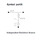
Use "analogLib/port3t" where you have to set C and L value.

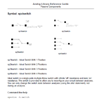
Or use Analysis dependent Switch, "analogLib/sp1tswitch".

I don't recommend "analogLib/port3t".
I recommend "analogLib/sp1tswitch".
 

Attachments

  • 160519-015532.png
    160519-015532.png
    39.4 KB · Views: 154
  • 160519-015631.png
    160519-015631.png
    6.1 KB · Views: 176
Last edited:

So, basically if I plot the Gmax and ask for the value when it crosses the 0db axis I get the fmax of the mosfet?

The port3t is like a 3 port element with on the left a switch, below a switch with a source like psin (sort of) and on the right is just a simple pin. I can use that instead of using capacitors and inductors?
 

So, basically if I plot the Gmax and ask for the value when it crosses the 0db axis I get the fmax of the mosfet?
Yes.

The port3t is like a 3 port element with on the left a switch, below a switch with a source like psin (sort of) and on the right is just a simple pin. I can use that instead of using capacitors and inductors?
port3t is no more than combination of port, capacitor and inductor.
It is not switch.

Again surely read my append.
 

Sorry. Gonna read and get back in 5 minutes with the sim results.

- - - Updated - - -

Sorry. Gonna read and get back in 5 minutes with the sim results.

But tell me, how am I supposed to use only one switch and make it open in DC AC etc?
 

But tell me, how am I supposed to use only one switch and make it open in DC AC etc?
Use four sp1tswitch.
Two switches are for gate.
Another two switches are for drain.
One switch is for bias.
The other is for port.

Or use two sp2tswitch.
One is for gate.
The other is for drain.
 
Last edited:

I see, and on those switches I have to configure the positions for each analysis.

For the gate I put:

The sw to the psin source switch position 0, DC position 0 and AC postion 1. The other switch to the bias I put: switch position 1, DC position 1 and AC postion 0.

For the drain:

The sw to the psin source switch position 0, DC position 0 and AC postion 1. The other switch to the bias I put: switch position 1, DC position 1 and AC postion 0.

I get a very stange plot:

**broken link removed**

Attention: My transistors are not RF Transistors.
 

**broken link removed**


log x

**broken link removed**

- - - Updated - - -

By the way pancho, what I am trying to do is verify in which frequency range at which the mosfet model is valid. Is this a good way?

- - - Updated - - -

I have increased the frequency for the simulation up to 500GHz and the curve never crosses the 0 db axis.

- - - Updated - - -

It crosses at 952Ghz.

- - - Updated - - -

kf and Gmsg

**broken link removed**
 
Status
Not open for further replies.

Part and Inventory Search

Welcome to EDABoard.com

Sponsor

Back
Top