Continue to Site

Welcome to EDAboard.com

Welcome to our site! EDAboard.com is an international Electronics Discussion Forum focused on EDA software, circuits, schematics, books, theory, papers, asic, pld, 8051, DSP, Network, RF, Analog Design, PCB, Service Manuals... and a whole lot more! To participate you need to register. Registration is free. Click here to register now.

frequency response od LDO circuit

Status
Not open for further replies.

perado

Full Member level 2
Joined
May 28, 2010
Messages
127
Helped
2
Reputation
4
Reaction score
2
Trophy points
1,298
Activity points
2,134
why we should draw frequency response for open-loop circuit in LDO that uses feedback?
Isnt true that draw this for feedback circuit?
what I should do to draw frequency response of a LDO circuit?
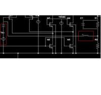
 

The most important frequency response of for the LDO circuitry is the magnitude/phase characteristic of the complete open loop (including all parts which are part of the loop). This simulation is necessary for evaluating the stability properties after closing the loop.
 
  • Like
Reactions: perado

    perado

    Points: 2
    Helpful Answer Positive Rating
It is a negative feedback. Suppose open loop gain is A(s) and feedback factor is -1. Close loop gain is H(s). Input signal is vi and output signal is vo.
Then calculate H(s).
(vi-vo).A(s)=vo
so, H(s)=vo/vi=A(s)/[1+A(s)]
If A(s)=-1, H(s) will be infinite. It means unstable.
So we can analyze open loop gain A(s) to obtain close-loop stability.
 
  • Like
Reactions: perado

    perado

    Points: 2
    Helpful Answer Positive Rating
thanks for your reply
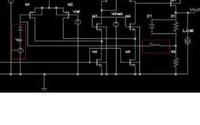
I break the feedback for open-loop ac simulation , I put an inductor and a capacitor series with ac-source as shown in picture
Is it true for acheive frequency response? what value is suitable for inductor and capacitor?
with this procedure DC-gain is equal to 0dB , because inductor is short circuit and then Vo is equal to Vi, but frequency response of LDO in papers is different, how I can solve this problem in y simulation?


I can not see your image, but your description sounds wrong. The inductor should provide a dc path, but an AC open. It should be in in series with the feedback path. The capacitor should be at the point of feedback to the error amplifier to provide an AC ground. The AC signal should be at the reference input. 1F and 1H should be good values.
 
  • Like
Reactions: perado

    perado

    Points: 2
    Helpful Answer Positive Rating
I break the feedback for open-loop ac simulation , I put an inductor and a capacitor series with ac-source as shown in picture
which picture?

Is it true for achieve frequency response?
Yes.

what value is suitable for inductor and capacitor?
Big values, like e.g. 1H & 1F.

with this procedure DC-gain is equal to 0dB , because inductor is short circuit and then Vo is equal to Vi, but frequency response of LDO in papers is different, how I can solve this problem in y simulation?

Use your standard feedback configuration -- e.g. resistive voltage divider feedback to the inverting input -- break the loop between the voltage division node and the inverting input, there between insert the LC lowpass and a unit AC source in series (or an iprobe in C@dence ADE). Measure the output voltage before the LC lowpass, i.e. at the voltage divider node. By this you should measure your actual DC gain.
 
  • Like
Reactions: perado

    perado

    Points: 2
    Helpful Answer Positive Rating
Sorry I had attached but I dont know what happened for it!!
Now I attached it again and please help me respect to it
I think upload center has problem because now the image is in my last post
 

The Cap should be connected to an AC gnd, like GND. The AC stimulus should be applied at vref.
 
  • Like
Reactions: perado

    perado

    Points: 2
    Helpful Answer Positive Rating
The Cap should be connected to an AC gnd, like GND. The AC stimulus should be applied at vref.
Actually both methods can work. I'd personally prefer perado's method as the crossover frequency can easily be identified at 0 degrees.
 
  • Like
Reactions: perado

    perado

    Points: 2
    Helpful Answer Positive Rating
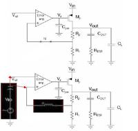
Thanks for your replies , but I dont answer my question , maybe my question isnt clear , I ask it again clearly at the picture that I attach here at the top circuit schematic close-loop LDO circuit is shown and in the bottom its my procedure for simulate open-loop LDO circuit, I break feedback but for provide DC bias of transistor I put a large inductor (Is it true?) and now for AC simulation, ac-voltage source connect to which point? ( + node or - node of error amp? ) on the other hand where is Vi? if I select (+) as Vi then dc-gain be one and it isnt correct.


Yes it is true. To get the correct bias point you use an inductor to break the feedback loop. The AC source should be applied to -("vin vref 0 1.22 AC 1"). The cap should be at + to GND. The reason is your input is vref. The gain is vref/vout. You want the + input to be at AC ground, hence the large cap to gnd.
 
  • Like
Reactions: perado

    perado

    Points: 2
    Helpful Answer Positive Rating
Perado - the loop should be broken with the aim to inject a test signal. Therefore, it is not correct to connect the ac source to the inverting input. Instead, feed the test voltage via a very large capacitor into the non-inv. input.
 
  • Like
Reactions: perado

    perado

    Points: 2
    Helpful Answer Positive Rating
LvW- I think your idea is agree with the open-loop circuit gain simulation set up that there are at the page24 of this thesis : **broken link removed**
but I have a question if I do it , then at low frequency or better in dc inductor is short circuit and capacitor is open-circuit then DC gain(Vo/Vi) will be 1 (0dB) , but itsnt in agree with open-loop simulation result in journal papers , then what I do?
 

perado, you are right, but don`t worry about it.
Of course, at very low frequencies and dc you cannot get correct results - however, the main purpose of simulating/evaluating the loop gain is to watch the behaviour for higher frequencies, in particular around a magnitude of 0 dB.
In case you want correct results also for very low frequencies you have to apply other methods (Middlebrook, double injection techniques). But, for my opinion, that is not appropriate in this case.
 
  • Like
Reactions: perado

    perado

    Points: 2
    Helpful Answer Positive Rating
... then DC gain(Vo/Vi) will be 1 (0dB) , but itsnt in agree with open-loop simulation result in journal papers , then what I do?

Perado: if you just don't want to see the DC gain on a gain vs. frequency plot starting at - say - 1Hz, simply use a lowpass with a much lower frequency, say L=100H , C=100F ⇒ fo = 1/2π√(LC) ≈ 1.6 mHz ≪ 1Hz .
 
  • Like
Reactions: perado

    perado

    Points: 2
    Helpful Answer Positive Rating
An ideal circuit breaker will pass all DC values and reject all AC signals, down to DC.
So ideally, you need an ideal filter with a cutoff frequency at DC.
As erikl has stated, the cutoff frequency of your LC filter basically requires infinitely large inductors and capacitors.
So what you see is at extremely low frequencies are actually due to the non idealities of your isolation filter, and not a problem with the open-loop theory.

If you read your simulator user manual, ideal caps and inductors may have a DCCUT and DCFEED specification which can be used for creating ideal filters. Pr ypu can use other means like Middlebrook, which is the most accurate but computationally intensive method.
Of course, as LvW has mentioned, for most applications, we do not really need to care about the low freq errors caused by the non-ideal LC filter. And mostly, we do not need the accuracy of Middlebrook.
 
  • Like
Reactions: perado

    perado

    Points: 2
    Helpful Answer Positive Rating
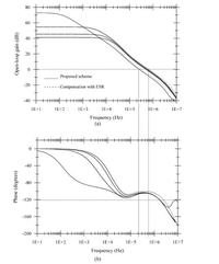
I agree with your comments but I saw in all of papers bode plot for open loop circuit like the picture that I attachad and I want to show bode plot like this for my circuit , note my simulator is ADS , then for this approach what method you recommend to me?
 

perado, there is only one alternative: AC analyses and display of the ratio loop_out/loop_in as magnitude (in dB) as well as phase.
 

The method is to simply start plotting at a frequency where the non-idealities of the isolation filter are negligible.
Eg. in the plot you had shown, the designer started plotting only from 10Hz onwards.
 

Status
Not open for further replies.

Similar threads

Part and Inventory Search

Welcome to EDABoard.com

Sponsor

Back
Top