Continue to Site

Welcome to EDAboard.com

Welcome to our site! EDAboard.com is an international Electronics Discussion Forum focused on EDA software, circuits, schematics, books, theory, papers, asic, pld, 8051, DSP, Network, RF, Analog Design, PCB, Service Manuals... and a whole lot more! To participate you need to register. Registration is free. Click here to register now.

Frequency domain of duty cycle

Status
Not open for further replies.

AlienCircuits

Member level 5
Joined
Jun 14, 2012
Messages
81
Helped
0
Reputation
0
Reaction score
0
Trophy points
1,286
Activity points
2,134
I am on the path of designing my first SMPS from scratch, and I have found that deviating from 50% duty cycle requires me to have faster switches (ft, bandwidth, whatever you want to describe their switching performance with). I have a suspicion about duty cycle and the maximum switching speed of my transistor, and I am wondering if anyone else already has the answer or if they at least agree or disagree with me.

I'll make a hypothetical example, and tell me if you agree or disagree with me. Say I pick a MOSFET with a maximum switching frequency of 100kHz. Now, if I switch it at 100kHz and try to deviate its duty cycle either below or above 50%, the switching signal will be degraded because for one half of the period, I will need to switch faster (in a shorter time) than the 10us period. I would not be able to achieve a duty cycle of 10%, for example, without a faster rated switch.

Does anyone have a figure for different duty cycles of PWM in the frequency domain? I know this must have been analyzed a million times be people in the past, and the modulation in PWM seems to imply that there must be some frequency effect. If no one gives me an answer, I will have to work this out myself.
 
Last edited:
You don't worry about a MOSFET's switching frequency in the frequency domain as such, you are concerned about its switching rise and fall times (which should be a small percentage of the waveform period for good efficiency). And since the switching time is generally determined by how fast you can charge and discharge the MOSFET gate, that is generally the critical parameter in operating a MOSFET as a switch. So for fast switching you want to look for a MOSFET with minimum gate capacitance (gate charge to switch) for the current you need to switch, to make it easier to rapidly turn the transistor on and off.
 
Alien, the only thing magical about 50% I recall in RF days was I tune the slicer to exactly 50% using the relative 2nd harmonic content level in the days when 2% loss of window margin for dat recovery was too much.

But for spectral content in dB the duty cycle does not affect the harmonics generated by the edges much, just the repetitive stuff between the edges changes levels on fundamental and the next few harmonics. THe total bandwidth on square pulses is easily 20x the PWM rate.

Crutchow is correct on the junction capacitance. in fact the MOSFETS are voltage controlled switches but in reality, you cant do much better than "an effective current gain" of x100 on a MOSFET switch and x10 on a bipolar switch when you start switching big AMP junctions. IGBT's are a bit better when it comes to high voltage and high current and cheaper for those applications. But watch for progress in MOSFETs to compete in Hi-Power low ESR solutions.

But it all comes down to pre-driver ESR, driver ESR, load ESR and effective current gain which affects efficiency and temperature rise.. the rise time T=Rs*C where Rs=ESR , so when ESR gets lower, T gets lower in ps, ns, or µs and the spectral emissions give designers a challenge to keep CE and the FCC happy with EMC design and egress testing.
 
Last edited:
Alien, the only thing magical about 50% I recall in RF days was I tune the slicer to exactly 50% using the relative 2nd harmonic content level in the days when 2% loss of window margin for dat recovery was too much.

But for spectral content in dB the duty cycle does not affect the harmonics generated by the edges much, just the repetitive stuff between the edges changes levels on fundamental and the next few harmonics. THe total bandwidth on square pulses is easily 20x the PWM rate.

Crutchow is correct on the junction capacitance. in fact the MOSFETS are voltage controlled switches but in reality, you cant do much better than "an effective current gain" of x100 on a MOSFET switch and x10 on a bipolar switch when you start switching big AMP junctions. IGBT's are a bit better when it comes to high voltage and high current and cheaper for those applications. But watch for progress in MOSFETs to compete in Hi-Power low ESR solutions.

But it all comes down to pre-driver ESR, driver ESR, load ESR and effective current gain which affects efficiency and temperature rise.. the rise time T=Rs*C where Rs=ESR , so when ESR gets lower T gets lower and the spectral emissions give designers a challenge to keep CE and the FCC happy with EMC design and egress testing.

My problem is that I have to use big amp junctions without passing big amps through. My design is to regulate 800V with about 150 uA load current. I have found that an impractical inductor size and impractically high switching frequency are needed to get into continuous mode, so I'm using discontinuous mode and am finding that actually lowering my frequency is giving me a lower frequency requirement in the low duty cycle switching region. I have been using f/D as a relationship to minimize in my Vo/Vi equation. For example, if duty cycle remained a constant 10%, then at f = 30kHz, the duty cycle 10% period is longer than the same 10% duty cycle period of f = 40kHz. I actually have this plotted, and can see the relationship. Since D is proportional to √f (bigger f gives less ratio of f/D), minimizing f by its square root minimizes f/D linearly. I am picking parts based on their Vds breakdown voltage because I am converting from 1000V. But, as a result, the only parts rated that high are also designed with huge junction capacitances.

With reference to what you said, if the fundamentals and a few harmonics are changing from the duty cycle effect, doesn't that mean that if the fundamental changes to a higher frequency that it will now fall outside the spec of the switching FET?

Also, you mention IGBTs might be better, but every where I have read to avoid IGBTs if a MOSFET can do the same job since they have higher frequency capability and lower power drop for low current applications.

Thanks to both of you for the responses and I like that you tied in the EMC aspect to this, because I haven't really thought that much about it even though I know I will probably face that challenge next.

- - - Updated - - -

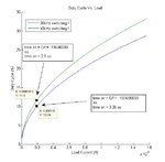
dutycycle.jpg

Here is what I mean, and I suppose its almost obvious. For the same load current, switching at a lower frequency actually gives me a longer on-time, even though the duty cycle decreases. So trying to increase f to buy a bigger D does not get you anywhere if you want to use a slower switch, and it actually hurts you since you must increase f proportional to its square to get a linear increase in D (and there is a constant factor related to the inductance, Vo/Vi, and load current).
 
Last edited:

I'm not able to recognize an actual problem addressed by your post. What do you e.g. mean by "fall outside the spec of the switching FET"?

There's no strict specification to be kept, except for voltage, current and power ratings. In your dedicated low power application, maximum voltage should be your main concern. With recent MOSFET, possible overvoltages will be silently absorbed by the controlled avalanche breakdown feature.

At low load currents, the required ton times will be most likely smaller than the achievable tr/tf values. Although switchings losses will increase considerably, you can still operate a switched mode converter in this range, particularly at low power.

High voltage IGBT speeds are lower by at least factor 10, so you won't want to use them for your application.

My regulator with large enough output caps will achieve this? As in, say my tr/tf values are too large so my switch is on longer than the regulator commanded it to be, and so after a few cycles my regulator will just command 0% duty cycle and this will balance out? If that is what you mean, then won't that introduce more ripple on my output? Also, I agree that max voltage ratings are my #1 determining factor that restricts all of my other choices. I have been considering the 1200V and 1500V MOSFETs, but I know that I'll be able to put some transient protection at the 1000V input so hopefully they will not see voltages much above 1000V.

As far as "fall outside the spec of the switching FET" , I think what I said equivalently translates to the tr/tf issue. Say I have 2 FETs, and one can switch at twice the frequency of the other with faster tr/tf, such that the deviation from a perfect square wave is the same for both (rise/fall time as a percentage of switching period). Then, the faster frequency switch will have better resolution for low duty cycle percentages when running at the same frequency as the slower switch. If I can lower my frequency enough that these high Qg/capacitance FETs look fast, I will increase my duty cycle resolution.
 
Last edited:

Rather than deriving theoretical duty cycle limits from FET specifications, why don't you check the behaviour of your switcher circuit with short ton times. A switch transistor isn't a logical circuit, it can still control current if not fully switched on or off. In every switched mode converter, the transistors are operating in linear range at least part of the cycle.
 
I accept what you say, but it scares me because I'm not sure how I would design a regulator to do both linear resistive control based on tr/tf and also switching PWM control simultaneously. Is the regulator solution more simple than that?
 

If you are using feedback control of output voltage, you don't need to care for theoretical duty cycles. That happens in any switched mode controller to a certain extent. During of the on-time, the switch transistor is in linear operation mode, generating additional switching losses. The feedback loop corrects the on-time, compensating for these effects.
 

If you are using feedback control of output voltage, you don't need to care for theoretical duty cycles. That happens in any switched mode controller to a certain extent. During of the on-time, the switch transistor is in linear operation mode, generating additional switching losses. The feedback loop corrects the on-time, compensating for these effects.

Alright, but since I have never designed a regulator for a SMPS, I am confused at how I would begin to model this to design my regulator on. I know how to design P/PI/PID controllers given transfer functions, but I'm not sure where I would even begin to get a transfer function for what you're suggesting. I have some papers on modeling SMPS circuits as linear circuits, but they are assuming the duty cycle is a perfect mathematical variable. I realize I may be able to just ignore these switching losses and let the regulator compensate for them, but I want to have accurate design choices for things like steady-state error and voltage ripple.
 

You should start the controller design with ideal switch parameters. Varying control system gain in DCM is already a kind of challenge. Non-ideal switch will mainly reduce the gain.

Or add a simple behavioral controller model to a Spice simulation and analyze the circuit work in closed loop operation.

Ah, I did not think that these losses would translate as a gain issue, but that makes sense. I think I could do non-linear modeling of the gain as a function of duty cycle percent or some other way to take it into account. I think I will try to digest what you've said and see if I can make some progress before posting any more questions. Thanks a lot.
 

Status
Not open for further replies.

Part and Inventory Search

Welcome to EDABoard.com

Sponsor

Back
Top