jincyjohnson
Member level 4
if we want get a pattern that is changed in ach clock cycle, how can we run in spartan 3E fpga kit. plz reply
Follow along with the video below to see how to install our site as a web app on your home screen.
Note: This feature may not be available in some browsers.
library ieee;
    use ieee.std_logic_1164.all;


    entity pattern_generation is
        port( clock : in std_logic;
              B_in  : in std_logic_vector(0 to 7);
              C_in  : in std_logic;
              pattern_out : out std_logic_vector(0 to 7) );
        end pattern_generation;


    architecture ar of pattern_generation is

        component Recon_JC is
        port(clk2 : in std_logic;
             rst  : in std_logic;
             mode_sel : in std_logic_vector(1 downto 0);
             Jn_in    : in std_logic_vector(0 to 7);
             Jn_cw    : out std_logic_vector(0 to 7)
             );
         End component;
        component accumulator_cell is
        port( clock    : in std_logic;
              set      : in std_logic_vector(0 to 7);
              reset    : in std_logic;
              c_in     : in std_logic:='0';
              B_in     : in std_logic_vector(0 to 7);
              Pattern  : out std_logic_vector(0 to 7) );
          end component;

        signal count_out : std_logic_vector(0 to 7);
        signal temp:std_logic_vector(0 to 7):="00000000";
        signal mode_sel:std_logic_vector(1 downto 0):="00";
        signal rst:std_logic:='1';
        --signal count:integer:=0;
        begin
            process(clock)
                variable count:integer:=0;
                begin
                    if rising_edge(clock)then
                        count:=count+1;
                        if rst='1'then
                            mode_sel<="00";
                            rst<='0';
                            count:=0;
                            elsif count=0 then
                                mode_sel<="10";
                                elsif count>=1 and count<=9 then
                                    mode_sel<="01";
                                    elsif count>9 then
                                        mode_sel<="10";
                                        count:=1;
                                    end if;
                                end if;
                            end process;


            S00: Recon_JC port map(clock,rst,mode_sel,temp,count_out);
            S01: accumulator_cell port map(clock,B_in,rst,C_in,count_out,pattern_out);

end ar;Bad idea making clocks from counters in the logic fabric. FPGA's have very limited access to the global clock buffers from the logic fabric. The placement of the clock driving flip-flop can vary from build to build unless you lock down the placement of that flip-flop. Even then the routing can vary depending on the placement of other logic around the area. The only time it might be a good idea is if it is the only clock used in a design and the input clock is only used to run the counter. This would still mean that the clock generated from the counter must be considered as asynchronous to the input clock and anything from outside the FPGA.The clock divider code is as follows
[/CODE]library IEEE;
use IEEE.STD_LOGIC_1164.ALL;
use IEEE.STD_LOGIC_ARITH.ALL;
use IEEE.STD_LOGIC_UNSIGNED.ALL;
entity c1 is
port ( CLKin: in std_logic;
reset: in std_logic;
CLKout: out std_logic);
end c1;
architecture arch of c1 is
signal counter: integer:=0;
signal temp : std_logic := '1';
begin
process(CLKin,counter,reset)
begin
if(reset='0') then counter<=0; temp<='1';
elsif(CLKin'event and CLKin='1') then counter <=counter+1;
if (counter = 12000000) then temp <= NOT temp; counter<=0;
end if;
end if;
CLKout <= temp;
end process;
end arch;[/code]
Oh, how I detest instantiated components done with positional associations, what happens if you change the order of the ports in the component declaration. Opps the design doesn't compile...jincyjohnson said:Code:S00: Recon_JC port map(clock,rst,mode_sel,temp,count_out); S01: accumulator_cell port map(clock,B_in,rst,C_in,count_out,pattern_out);
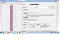
Did you read the user guide for the core. It tells you step by step what all the tabs and the items on those tabs mean.jincyjohnsom said:when the clock wizard is is open i got this screen. what are the next steps. plz reply.
Oh, how I detest instantiated components done with positional associations, what happens if you change the order of the ports in the component declaration. Opps the design doesn't compile...
") It will just give you a result that is completely wrong, and you will spend many hours wondering whyyyyyy, oh whyyyyyyy??!?
It will just give you a result that is completely wrong, and you will spend many hours wondering whyyyyyy, oh whyyyyyyy??!?This is worth repeating ... twice:Did you read the user guide for the core. It tells you step by step what all the tabs and the items on those tabs mean.