Continue to Site

Welcome to EDAboard.com

Welcome to our site! EDAboard.com is an international Electronics Discussion Forum focused on EDA software, circuits, schematics, books, theory, papers, asic, pld, 8051, DSP, Network, RF, Analog Design, PCB, Service Manuals... and a whole lot more! To participate you need to register. Registration is free. Click here to register now.

flyback transformer noise

Status
Not open for further replies.

tictac

Full Member level 5
Joined
Oct 22, 2006
Messages
297
Helped
3
Reputation
6
Reaction score
3
Trophy points
1,298
Location
Polland
Activity points
3,572
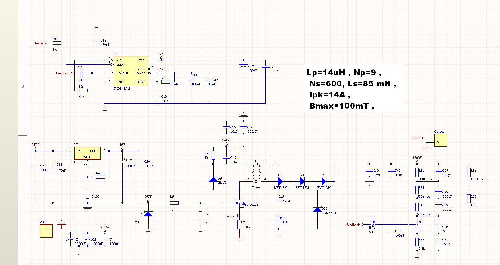
I made a DC-DC flyback converter and it worked.it has a variable output voltage. But at some of the voltage range the transformer makes loud noise. The switching frequency is 50khz. it work in discontinuous mode and I use UC3842 for controller. I guess that I have oscillation at feedback loop. I check pin 1 of 3842 with scope. at normal state there is a dc voltage at pin 1 but having been a buzz heard, a 1khz sinus of waveform will emerged at the pin1 of uc3842 .

in order to improve the noise,I connect the fairly large cap across the feedback network(up too 100nf) inspite of this effort, the noise will not be vanished.

I have a low pass filter on pin 3(1K resistor and 470p cap) when I connect a larger cap (such a 1nf) to pin 3 the noise will be better .
but still,I have buzz on some of voltage range.

how Can I Vanish the buzz wholly?

Regards
 

Re-calculate the feedback loop compensation and adjust it, if necessary.
 

    tictac

    Points: 2
    Helpful Answer Positive Rating
is there anybody to help me? I must improve it fast

Regards
 

Without knowing the transformer primary inductance and winding ratio, the compensation can't be exactly calculated. But
most likely, the feedback compensation capacitor C7 is much too large. A typical dimensioning is rather 100 pF. Your control process
has already a pole created by the output capacitor. Adding a second pole of similar time constant to the loop reduces the
controller's phase margin to about zero.

Why don't you post your schematics at edaboard, by the way?
 

    tictac

    Points: 2
    Helpful Answer Positive Rating
Thank you for reply :)
Lp=14 uH Ls=97mH Ipk=14A, Bmax=100mT, f=50khz
is it true?


I calculate The value for Capacitance at output about 10nf for 40mA load .but for reducing the output ripple I increase the value of capacitances. do you mean that should I reduce the output capacitance value(for example 22nf)?


Adding a second pole of similar time constant to the loop reduces the
controller's phase margin to about zero.
can you describe it a little more,please? is it cause of the oscillation at feedback loop?

regards
 

can you describe it a little more,please? is it cause of the oscillation at feedback loop?
Yes, I think so. Simply try to reduce C7, as said.
 

    tictac

    Points: 2
    Helpful Answer Positive Rating
Hi FvM

I try C7 with 100pf, 150p,330p with R2=150k , 100k
but the buzz was louder.
I try C12 with 1nf and it was better but still having the buzz.
I had read that increasing the C12 may be Added another pole!!

Can I reduce the value of C39 and C40 at output? is it effective?

Can you guide me,please?

Regards
 

I doubt, if the problem can be understood by only analysing the circuit, it may be a problem of non-ideal behaviour. In any case,
I would try to achieve a stable operation by further reducing the feedback gain.

Basically, an inverter should be operatable with any capacitive load by adjusting the feedback loop.
 

    tictac

    Points: 2
    Helpful Answer Positive Rating
I would try to achieve a stable operation by further reducing the feedback gain.

Can you tell me how to reducing the feedback gain,please?and thanks you for the time spend for me.

Now,I increase the value of C12 to 22nf 8O (I know its unusual)
and the buzz has been vanished but I only have the buzz at 560v to 700v.

I suggest that there is a parasitic inductance in current sensing path(Maybe).
when the C12=470pf the drain waveform of mosfet included one period of sinus waveform at off time of mosfet switching, but when I increase C12, It was more like a square wave

is it good solution to reduce the buzz or should I adjust the feedback gain or improve grounding for pcb or reduce tracks lenght of pcb further or...????


Regards
 

"parasitic inductance in current sensing path" is one of the possible non-ideal circuit behaviour cases I imagined. It can be
mainly determined by inspecting the individual waveforms, but may be hard to identify in detail.

Stronger low-pass filtering of the current sense would be O.K. if the basic current controlled PWM operation is still maintained. I fear,
it's not the case with 22 nF and 50 kHz PWM frequency. Apart from possible unwanted signals due to parasitic inductances, you
have most likely a problem of the high and varying PWM gain in discontinuous operation. Also resonances of transformer leak
inductance and secondary winding capacitance may further complicate the situation.

As an interesting question, is the PWM operating stable in non-feedback mode, when supplying a constant signal to the error amplifier?
You should still get a constant (but unregulated) output voltage by current mode. If this mode basically achieves a constant PWM without
"noise", the circuit should be operatable at low feedback gain as well. A low feedback gain without loosing load regulation can be
accomplished by using a PI circuit, e.g. the original C7 of 100 nF with a series resistor that sets the gain.
 

    tictac

    Points: 2
    Helpful Answer Positive Rating
The 1250V waveform raises some basic doubts about correct operation of your circuit.

You have an unstable operation with alternating long and short on-time. Ignoring the possible reason for a moment, you also see this:
The on-time is about 10 us, resulting in 17 A peak current. Considering rDSon, current sense resistor and winding resistance, it's a
bit lower, e.g. 14 A. It gives 1.3 mWs stored energy, respectively 32.5 W average power with 25 kHz repetition. Did you
connect a higher load? If not, where's the power dissipated?

Another surprizing point is the Vds waveform. Either something is wrong with the measurement, or the supply voltage is not
constant 24V. Very simple, Vds average value can't be different from about Vb.
 

    tictac

    Points: 2
    Helpful Answer Positive Rating
Now,I increase the value of C12 to 22nf (I know its unusual)
and the buzz has been vanished but I only have the buzz at 560v to 700v.

after I increase C12 , after some times, 3 output diode (byt43m) was burn.at First I didnt understand the problem and I mixed up about 4 hours. :(

now I back to first state with buzz and oscillation.


Also resonances of transformer leak
inductance and secondary winding capacitance may further complicate the situation.

how Can I reduce transformer leak inductance? I use one copper sheild between primary and secondary winding and another copper shield on outer winding and ground them(to reduce parasitic cap).


As an interesting question, is the PWM operating stable in non-feedback mode, when supplying a constant signal to the error amplifier?

At first I test 3842 in non-feedback state and pwm was constant but now its variable. one of my friend told me that in flyback with current mode and with 3842, its a normal mode that you have two different duty cycle of pwm and the average of this two different pwm is the main duty cycle.is it true? Can you tell me how to get constant pwm with feedback,please?


If this mode basically achieves a constant PWM without
"noise", the circuit should be operatable at low feedback gain as well

but now, I still have a noise :( what can I do? so low feedback gain will cancel?

Regards
 

one of my friend told me that in flyback with current mode and with 3842, its a normal mode that you have two different duty cycle of pwm and the average of this two different pwm is the main duty cycle.is it true?
As far as I understand (and experienced), it's only true in continuous mode. In this case a special circuit extension, called
slope-compensation (see the 3842 application notes for details) is needed. But in discontinuous mode, the instability can't be explained by
current mode basic behaviour.

Regarding leak inductance, I didn't mean that it causes the problems. It may additionally complicate the circuit behaviour.
But it has to be accepted in some circuits.

As said, your circuit's behaviour isn't completely clear to me. I fear, I can't understand it fully from a distance.
 

    tictac

    Points: 2
    Helpful Answer Positive Rating
But in discontinuous mode, the instability can't be explained by
current mode basic behaviour.
I see slope compensation in one article from Dr. Ridley and as you say its for continuous mode.
So,how Can we get constant pwm in discontinuous mode?


As said, your circuit's behaviour isn't completely clear to me. I fear, I can't understand it fully from a distance.

is there anything that I didnt tell you about this circuit? is the pcb of the circuit help for better understanding?Sorry that I was disturbing you but this project is very important for me and I work on this project for several months but still it has some problems.

Regards
 

I didn't mean, that you kept essential information. But it's simply difficult to debug a circuit by remote diagnosis.
 

    tictac

    Points: 2
    Helpful Answer Positive Rating
Can we check each part of the converter step by step? for example start from transformer? was it help? I have enough time(about 1 month) to complete it. if you have a little time and agree with me.
anyway,thanks you so much for these valuable information that you teach me.

regards
 

I'm not sure about the chances. Getting local help would be more promising. But I can try to help you further. There are two points
from by previous posts, that aren't clearly answered in my opinion - or I didn't understand the answer correctly.

The first is about behaviour in open loop operation. (you have to care to limit the output voltage in this case). Is it stable or not? I
understood from your previous post that it's undstable as well. Then the problem wouldn't be related to feedback compensation at all.
If it's stable (at all output voltage levels) however, than a stable low gain feedback compensation is possible too.

The second point is about the explanation of the Vds waveforms you showed. As said, they seem to contradict a constant 24V supply.
It would be interesting to see the output waveforms as well. A 100:1 high voltage probe or a selfmade compensated divider would
be necessary to see it.
 

    tictac

    Points: 2
    Helpful Answer Positive Rating
thanks you for helping

At first I test 3842 in non-feedback state and pwm was constant .

the supply voltage is about 26 volt(because the supply voltage will be 2X12v battery ) and RL=49k and when I see supply voltage with the scope I see one AC over voltage or spike with 50khz frequency and with 0.5 volt amplitude.

I put R36 and R37 on the circuit to seeing output voltage waveform with scope.is it a good way to see high voltage waveform or not? it has about 6 volt ripple per 1250 volt.

I will post the picture of this waveform at edaboard as soon as possible.

at my first pcb the Gnd of High current is connected to the Gnd of controller and it was causing many problem such a 30 volt ripple at output and 2 volt spike at supply voltage. but now I have two different path for Gnd of high current and controller. and I try to reduce stray inductance of the tracks by having short and wide track(but I dont know how much I was succeed?)


regards
 

Status
Not open for further replies.

Similar threads

Part and Inventory Search

Welcome to EDABoard.com

Sponsor

Back
Top