Continue to Site

Welcome to EDAboard.com

Welcome to our site! EDAboard.com is an international Electronics Discussion Forum focused on EDA software, circuits, schematics, books, theory, papers, asic, pld, 8051, DSP, Network, RF, Analog Design, PCB, Service Manuals... and a whole lot more! To participate you need to register. Registration is free. Click here to register now.

Flyback SMPS with primary clamp that is far too small?

Status
Not open for further replies.
T

treez

Guest
Hello
We have had a 100W Boundary Conduction Mode flyback LED driver SMPS designed for us by a consultancy and we believe they have messed up. What do you think?.....

The flyback is connected to the 420V output of a preceeding boost PFC stage.

The flybacks spec is….
Vin=420V
Vout=40V
Iout = 2.5A
L(pri) = 520uH
NP/NS = 3.2
F(sw) = 75KHz
Peak primary current at max load is 2.2A

Unfortunately I do not have the transformer spec, the consultancy are keeping this to themselves.
I do not know what is the leakage inductance in the transformer.

The problem is that the primary clamp/snubber consists of just an ES1J ultra fast diode feeding into a SMB size, 220V TVS. The TVS is on minimal pads. The TVS part number is SM6T220A

This seems miles too small for a 100W flyback.

Supposing that the leakage inductance was 1% of primary, ie 5.2uH, then…

The power dissipated due to the leakage inductance is 0.5*5.2e-6*(2.2^2) * 75000 = 950mW….however….
Since some of the flyback’s power current ends up unfortunately flowing into a flyback primary clamp, the power dissipation in this SMB TVS will be more than this.

Would you agree that a single 220V SMB size TVS is miles too small for the primary clamp of a 100W flyback as described?

ES1J diode datasheet:
https://www.fairchildsemi.com/datasheets/ES/ES1J.pdf

SM6T220A TVS datasheet
**broken link removed**

The flyback switching FET is FCPF1300N80Z (800V TO220 FET)
 
Last edited by a moderator:
Once we designed a 40 W flyback converter. It was controlled by a PFC controller IC (FAN7527B). We made several tests, and the best thermal result was combining both RC clamp plus a 250V TVS, which has a big THT package (P6KE250A).

I don't know what others think about, but for my experience this SMB package is small for this application. I studied a lot of commercial supplies of the same kind, and most of them used THT diodes for clamping, even for lower power ratings like 40, 50 or 60 W. The manufactures also give 5 years warranty, so they don't save on this parts.

About the leakage inductance, it is often said that it should be less than 2% of primary inductance. But it is common for it to reach 3%, which increases clamp's dissipation.
 
  • Like
Reactions: treez

    T

    Points: 2
    Helpful Answer Positive Rating
Vin=420V
Vout=40V
Iout = 2.5A
L(pri) = 520uH
NP/NS = 3.2
F(sw) = 75KHz
Peak primary current at max load is 2.2A

To the consultants, it may be about saving a few pennies. Perhaps they believe their device can safely clamp a higher V at low A, rather than needing to design a snubber for lower V at greater A. Because a normal snubber would need to dissipate several tens of W.

Looking at the specs...

Your turns ratio spec is not the same as would be expected from dividing Vin / Vout. As a result, a shorter duty cycle is required (in the area of 25%).

It is customary to design a flyback for 50% duty cycle.
Raw calculations would result in a turns ratio of 10:1. (Suitable for 420 V in, 40 V out.)

The shorter duty cycle tends to create current flows, and volt levels, that are not typical of your everyday flyback.

My knowledge is incomplete, thus this post is worth what it cost.
 
  • Like
Reactions: treez

    T

    Points: 2
    Helpful Answer Positive Rating
Thanks, but sorry, the duty cycle of a flyback doesnt need to be 50%....in some cases maybe yes, but not always, and certainly not generally. If you think of a diode duty cycle and the fet duty cycle, , then generally the one with the longer duty cycle is the one with the more current in it...but their are other considerations, such as, you may want to keep your primary peak current down so as to reduce the loss due to the leakage inductance.....in this case you would make the fet duty cycle a bit longer.

Also, it would not be 10's of watts of loss due to the leakage inductance....unless of course the leakage inductance was really large.

And As you know for a flyback in ccm, the conversion ratio is vout/vin = n.d/(1-d)
where
n = ns/np
d = duty cycle (fet duty cycle)
 

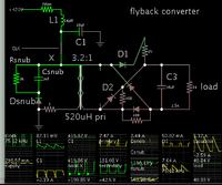
Here is my simulation, for comparison purposes. I certainly would not dispute your statements.

You're correct that the snubbing network averages around 6W worth of heat dissipation.


I thought up another theory about the consultants' decision to use a snubbing TVS:

They may have designed transformer operation to create a predictable voltage range...

So that the TVS (a) activates only when voltage rises to a high enough level, and (b) conducts only briefly while voltage is above that level, and (c) carries miniscule Amperes when it conducts.

Hence they designed it so the TVS has an easy job to do. Perhaps it will not have its useful lifetime reduced.

------------------------------

My observations about the turns ratio:

The 3.2 turns ratio causes the secondary to generate 131 V (420V divided by 3.2). This suggests the secondary has more turns than necessary.

If D1 were present, and conducting fully, tens of Amperes would come from the secondary during the 'on' cycle. However there is no diode in that position in a normal flyback.

My simulation shows the design can work. There is an advantage in having a 25% duty cycle, since there is adequate room to lengthen it if desired, to obtain greater output power.
 
  • Like
Reactions: treez

    T

    Points: 2
    Helpful Answer Positive Rating
As you know, 131V is the voltage reflected to the secondary when the primary is conducting.
The secondary has that number of turns so as to keep the secondary duty cycle longer

vout/vin = n.d/(1-d)

n=ns/np
d = duty cycle

this is the ccm equn but applies to BCM to as BCM as CCM in the limit
 

The np/ns of the present design is that of a typical wide range off-mains SMPS. It's expected to work over a e.g. 90 - 240 or whatsoever input voltage range.

I must confess that I don't understand what's the problem presently discussed in this thread. You have initially asked about snubber power dissipation, and it seems to me that the calculation is basically right. So what's the outstanding question?

If none (or not related to the question title), the thread should be marked as solved.
 
  • Like
Reactions: treez

    T

    Points: 2
    Helpful Answer Positive Rating
The question is, is one (SMB size) TVS capable of handling the heat it will take when used as a primary clamp for this flyback smps?
I know it depends on the leakage inductance, but the consultant wont tell us this...he gave the transformer design to a transformer manufacturer and we then just order it off them...but we cant get any at the moment
 

Also, it would not be 10's of watts of loss

Want to clarify... It was my own simulation which showed tens of W burden on the snubber network. Turns ratio 10:1. 50% duty cycle. Transformer primary is 2mH.

Theoretically, of course. It's the snubber's job to dissipate the surge which emerges from the primary after each power cycle. Since the primary carries a peak greater than 100 W, then it is reasonable for the snubber to have tens of W burden on it.

However your consultancy appears to have designed things so that they reduce the burden on the snubber. It is more efficient, and draws less average Amperes from the supply than my layout does. My values are based on 50% duty cycle, and zero Amperes trying to go through D1.

Nevertheless I can't help thinking that they made tradeoffs somewhere.

Example, since the secondary produces over 100V, then you start to lose the advantage of an isolated secondary.
 
  • Like
Reactions: treez

    T

    Points: 2
    Helpful Answer Positive Rating
Example, since the secondary produces over 100V, then you start to lose the advantage of an isolated secondary
thanks yes , good point, though we hope that we can keep the 100v+ bit away from the fingers of the customer, at least its isolated, ie isolated away from mains transients
 

The question is, is one (SMB size) TVS capable of handling the heat it will take when used as a primary clamp for this flyback smps?
I know it depends on the leakage inductance, but the consultant wont tell us this...he gave the transformer design to a transformer manufacturer and we then just order it off them...but we cant get any at the moment
As I said, you calculation looks basically correct, and I agree that it's preferable to have a higher power dissipation margin for the TVS diode. In a real converter, part of the stored leakage inductance energy would be burned in the MOSFET, slightly unloading the TVS diode.

I see, that 1 % leakage inductance is just a guess. For a quantitative estimation, you can refer to the formulas in Snelling Soft Ferrites, or compare with transformers of similar geometry.
 
  • Like
Reactions: treez

    T

    Points: 2
    Helpful Answer Positive Rating
You'll soon know when you power it up and measure the TVS temp...! get a build sheet and make a Tx to test...
 
  • Like
Reactions: treez

    T

    Points: 2
    Helpful Answer Positive Rating
interesting thing is that the TVS is sited under the transformer, so the consultant may well have missed it when he scanned over the smps with his thermal camera.
 

Well pretty simple to ask them to measure it with a fine thermo-couple at full load...!
 
  • Like
Reactions: treez

    T

    Points: 2
    Helpful Answer Positive Rating
Status
Not open for further replies.

Similar threads

Part and Inventory Search

Welcome to EDABoard.com

Sponsor

Back
Top