T
treez
Guest
Hello,
We have got a contractor to do a 100W flyback led driver for us, and we believe that he has not done a very good job. The circuit works but we believe that its performance is compromised in the way that he has done it.
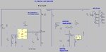
The circuit schematic and LTspice simulation are attached.
He has used an external current sense error amplifier with a 0 to 5V supply, and strangly he has used ground as the reference voltage into this error amplifier.
His current sense signal is then going below ground as the current builds up, and he has biased this signal up so that the led driver is in regulation when the inverting and non-inverting inputs of the error amplifier are both at 0V.
The problem is, the opamp’s negative supply is the 0V rail, and when the input to the inverting input of the error amplifier goes below zero, then the opamp does not “know” what this voltage is, because it is supplied from a 0 to 5V supply.
So what I am saying is that the opamp will not respond as strongly as it might to the feedback signal going too high negatively. The feedback circuit in this setup means that the opamp will not be as able to develop sufficient over-drive in order to regulate against higher-than-wanted LED currents.
Do you agree?
We have got a contractor to do a 100W flyback led driver for us, and we believe that he has not done a very good job. The circuit works but we believe that its performance is compromised in the way that he has done it.
The circuit schematic and LTspice simulation are attached.
He has used an external current sense error amplifier with a 0 to 5V supply, and strangly he has used ground as the reference voltage into this error amplifier.
His current sense signal is then going below ground as the current builds up, and he has biased this signal up so that the led driver is in regulation when the inverting and non-inverting inputs of the error amplifier are both at 0V.
The problem is, the opamp’s negative supply is the 0V rail, and when the input to the inverting input of the error amplifier goes below zero, then the opamp does not “know” what this voltage is, because it is supplied from a 0 to 5V supply.
So what I am saying is that the opamp will not respond as strongly as it might to the feedback signal going too high negatively. The feedback circuit in this setup means that the opamp will not be as able to develop sufficient over-drive in order to regulate against higher-than-wanted LED currents.
Do you agree?