Continue to Site

Welcome to EDAboard.com

Welcome to our site! EDAboard.com is an international Electronics Discussion Forum focused on EDA software, circuits, schematics, books, theory, papers, asic, pld, 8051, DSP, Network, RF, Analog Design, PCB, Service Manuals... and a whole lot more! To participate you need to register. Registration is free. Click here to register now.

[SOLVED] first layout - hot n-well problem

Status
Not open for further replies.

serhannn

Member level 4
Joined
Sep 28, 2010
Messages
69
Helped
2
Reputation
4
Reaction score
2
Trophy points
1,288
Activity points
1,939
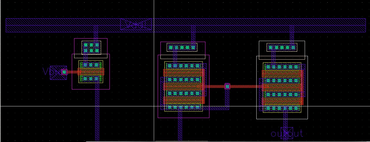
I've been trying to do the layout of a differential amplifier as my first layout. I fixed all the DRC errors, but "hot n-well". I know that it means the n-well is not connected to vdd, but in my case I think I connected it to vdd as you can see in the attached image..Is there something that I overlook or should I do something else to fix the error? By the way, I know my layout is very bad, I don't know any design rules or anything for now, so don't mind the gap between the transistors, etc.
Thanks a lot.


Hi serhannn,

Please when posting a DRC/LVS/QRC error you should be more specific,that is you should show the exact error given by assura/calibre etc...For your case,i think that you should create a n-well contact ring around your pmos transistors and then connect this ring to Vdd.Give it a try and see if this corrects the error.

N-Well contacts can be found from library manager as all other technology components and you should cover all of the ring with metal M1 and then connect it to Vdd.You should also leave the ring "broken" wherever you want and not "close" it as a real ring.

Regards,
Jimito13
 

jimito13, thanks for your reply. Next time, I'll try to be more specific; the error I get her is exactly: "INFO: hot nwell" and I get if for all 3 transistors seen in the upper part of the image.
I don't think I understood what you mean in your reply. I already put some N_DC contacts near the PMOS transistors and I connected those to Vdd? Why should I create a n-well contat ring around my PMOS transistors in this case. Also, I didn't really get what you mean by saying that I should leave the ring "broken"..
 

Never mind, I solved the problem. It turned out that I made a mistake and used MET1-pin instead of Pin-M1 while labeling VDD and gnd.. That's why I was getting the hot nwell warning. Thanks anyway.
 

Status
Not open for further replies.

Part and Inventory Search

Welcome to EDABoard.com

Sponsor

Back
Top