Continue to Site

Welcome to EDAboard.com

Welcome to our site! EDAboard.com is an international Electronics Discussion Forum focused on EDA software, circuits, schematics, books, theory, papers, asic, pld, 8051, DSP, Network, RF, Analog Design, PCB, Service Manuals... and a whole lot more! To participate you need to register. Registration is free. Click here to register now.

FINFET BASED DIFFERENTIAL AMPLIFIER

Status
Not open for further replies.

MOHAMMAD ALEEM

Junior Member level 2
Joined
Feb 9, 2021
Messages
20
Helped
0
Reputation
0
Reaction score
0
Trophy points
1
Activity points
133
I have designed a finfet based self biased differential amplifier .Amplifier without feedback is working fine but giving distorted result with both capacitive and resistive feedback using HSPICE. Any possible reasons?
 

Attachments

  • finfet amplifier.txt
    21.6 KB · Views: 100
Last edited:

Hi,

do you have a question?

Klaus
 

I think a schematic and some simulation results will be helpful.
 

I think a schematic and some simulation results will be helpful.
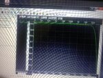
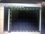
I am posting two snaps.one with gain of 2 with open loop amplifier and one with .13 gain with feedback resistor on inverting terminals .
 

Attachments

  • IMG_20210406_223844.jpg
    IMG_20210406_223844.jpg
    4.8 MB · Views: 100
  • IMG_20210406_223643.jpg
    IMG_20210406_223643.jpg
    3.7 MB · Views: 111

You say you get distorted results and yet you only show AC response. And still no schematic. If you want some one to help you, then help him/her help you.
 
sorry for all the inconvenience as i am new to the group.my schematic and graphs are posted here.I have applied 2.5 common mode voltage for biasing at input but in transient graph inpiut voltage is showing as 3.4754 volt but if without feedback then this voltage is accurately 2.5v with sinusoidal swing .
 

Attachments

  • IMG_20210407_093700 (1).jpg
    IMG_20210407_093700 (1).jpg
    6.3 MB · Views: 108
  • IMG_20210407_093700.jpg
    IMG_20210407_093700.jpg
    6.3 MB · Views: 108
  • IMG_20210407_094409.jpg
    IMG_20210407_094409.jpg
    3.9 MB · Views: 114
  • IMG_20210407_093700.jpg
    IMG_20210407_093700.jpg
    6.3 MB · Views: 109
  • IMG_20210407_094409.jpg
    IMG_20210407_094409.jpg
    3.9 MB · Views: 96
  • IMG_20210407_094422.jpg
    IMG_20210407_094422.jpg
    4 MB · Views: 113
  • IMG_20210407_094336.jpg
    IMG_20210407_094336.jpg
    2.9 MB · Views: 127

Is it your intention to connect this circuit in a positive feedback configuration? Also, I'm not sure but is the DC component in your SIN voltage source 2.5V?
 

I don't know what finFET technology you're using but
the one I've been exposed to (GF LPP14/LPP12) will not
handle 2.5V even using the "EG" (thick oxide) devices.
 

Is it your intention to connect this circuit in a positive feedback configuration? Also, I'm not sure but is the DC component in your SIN voltage source 2.5V?
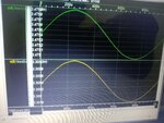
DC component i have used is Vdd+Vcc/2 and it is 2.5V .Problem is with 2.5V common mode voltage at both end i am getting gretaer then 2.5V at inverting terminal which is the common mode voltage applied.Also with feedback resistors i am not getting gain in ratio of feedback resistances.
 

I don't know what finFET technology you're using but
the one I've been exposed to (GF LPP14/LPP12) will not
handle 2.5V even using the "EG" (thick oxide) devices.
PTM 7 nm model i am using. Should i change the common mode voltage value?
 

Well, if you don't have a sine signal, just its common mode, then you will have 2.5V+2.5V if I read your netlist correctly. On the other input looks like you only have 2.5V.

You didn't say if you intentionally configured this circuit in a positive feedback.
 

Well, if you don't have a sine signal, just its common mode, then you will have 2.5V+2.5V if I read your netlist correctly. On the other input looks like you only have 2.5V.

You didn't say if you intentionally configured this circuit in a positive feedback.
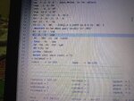
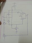
You can check the netlist.i have given both common mode and sinusoidal signal Vd. I just want to check my amplifier works as gain amplifier by giving feedback resistor R1 and R2 and checking dc gain which is not even close to R1/R2.How to sort out this issue?
 

Again. Didi you intentionally configured the amplifier in a positive feedback?

In addition there is 1.25V difference between the DC values of the two inputs. That's a huge offset.
 
Last edited:

Again. Didi you intentionally configured the amplifier in a positive feedback?

In addition there is 1.25V difference between the DC values of the two inputs. That's a huge offset.
I havent done it intentionally.Can you please tell me more how to be sure that applied feedback is negative or positive?
 

Well, it is easy. Your output is at 6 and node 5 is inverting because it is the input of inverter. 4 is then the non-inverting input.

But if you have that 1.25V difference in the DC bias between the two inputs, I don't know what this can cause. You have to simulate. Make the sine wave amplitude equal to 0 and see what happens.
When i am stimulating same circuit without feedback bias difference is 0.Might be feedback is adding some error.
 

Don't you have this from your netlist? Here the feedback resistors play no role.
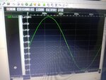
1617944565489.png
 

OK, something like the corrections I did in red

1618083121423.png
 

Status
Not open for further replies.

Part and Inventory Search

Welcome to EDABoard.com

Sponsor

Back
Top