Continue to Site

Welcome to EDAboard.com

Welcome to our site! EDAboard.com is an international Electronics Discussion Forum focused on EDA software, circuits, schematics, books, theory, papers, asic, pld, 8051, DSP, Network, RF, Analog Design, PCB, Service Manuals... and a whole lot more! To participate you need to register. Registration is free. Click here to register now.

FinFet 32nm invertor in Cadence

Status
Not open for further replies.

Annee

Newbie
Joined
Dec 21, 2020
Messages
1
Helped
0
Reputation
0
Reaction score
0
Trophy points
1
Activity points
7
We have been designing a finfet_32nm invertor in cadence as part of our research. However we are not getting the desired output
1608557539376.png

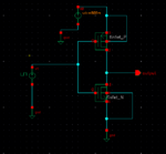
this is the invertor we designed. the out put we got is
1608557624980.png

we have currently given Vds values as 1V,0.6V,0.8V but none of these values also worked. Kindly suggest me wether there is an error in the design or the values we have provided

Thank you
 

Attachments

  • 1608557600410.png
    1608557600410.png
    21.9 KB · Views: 248

The plot is too washed-out to resolve much
numerically, but it appears that there is a
circuit discontinuity to me - the capacitive
looking glitch, and failure to ever go high.

I'd begin with sanity-checking the symbol to
SPICE pin and parameter-passing (like, is the
netlist order in the Cadence symbol putting
D, G, S, B (e?) in correct order to the netlist
line?).

Then, if you're sure connectivity is passed all
through the hierarchy correctly, try a pair of
N, P FET I-V sweeps looking for classical FET
ID-VD, ID-VG behaviors.
 

Status
Not open for further replies.

Similar threads

Part and Inventory Search

Welcome to EDABoard.com

Sponsor

Back
Top