cupoftea
Advanced Member level 5
Hi,
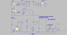
Why is the attached not the de facto method for Offline (post PFC) Two Transistor Forward?
(LTspice sim and jpeg attached)
It shows a heavily damped gate drive, which gains power from a pulse transformer hi side supply. The gate driver used is in fact a 2ED2109…a high voltage Bootstrap driver…..though you can note that its not used in Bootstrap mode. The fact is that the use of active electronics in hi side drive is severely non-recommended, so therefore, a chip that can handle the wildly changing B and E fields is needed…hence the 2ED2109…the best in the business.
Straight Bootstrap drives are just too dodgy for 400V input SMPS converters. This is well documented. Straight pulse transformer hi side drives are dodgy also…because there LC’s ring and can cause trouble…eg if gate drive very suddenly goes to zero duty, the ringing can bring a hi side FET on spuriously and cause shoot-through, or loss of transformer reset in some cases.
So why is the attached not more common…?...why are the semico’s not working on chipsets for this?