Continue to Site

Welcome to EDAboard.com

Welcome to our site! EDAboard.com is an international Electronics Discussion Forum focused on EDA software, circuits, schematics, books, theory, papers, asic, pld, 8051, DSP, Network, RF, Analog Design, PCB, Service Manuals... and a whole lot more! To participate you need to register. Registration is free. Click here to register now.

[SOLVED] Fail to write data from app_wdf_data signal to ddr3_dq_fpga(MIG,DDR3,Virtex 7)

Status
Not open for further replies.

rahdirs

Advanced Member level 1
Joined
May 22, 2013
Messages
424
Helped
93
Reputation
192
Reaction score
91
Trophy points
1,308
Location
Mordor
Activity points
4,492
Hi,
I have two doubts regarding writing data from app_wdf_data to ddr3_dq_fpga.I think,i followed the timing cycle for back to back write transactions given in ug586.

1) I am trying to write a sequence of (27'ha,27'hb,27'hc,27'hd,27'he,27'hf,27'hab,27'habc) from app_wdf_data to ddr3_dq_fpga.It is not getting written & some garbage values(222222,333333,999999 etc...) are getting written.

2) Ok,consider that garbage values in ddr3_dq_fpga which are getting written,when i try to read from ddr3,those values would be read out naturally.But those values are getting read in reverse order ?Why is this ?

Snapshot1:app_wdf_data
app_wdf_data.PNG

Snapshot2:ddr3_dq_fpga
ddr3_dq_fpga.PNG

Snapshot3:app_rd_data
app_rd_data.PNG
 

You sure it's not some endianness going on? Just ignore that for now, you have another problem...

Debug 101...You should trace the write into the DDR3 from the user interface side through the core to the DDR3 interface pins, as the core is writing "garbage" your user data is getting lost somewhere prior to the DDR3 interface, you'll have to find out where.
 

Hi,

It's not exactly garbage.My wording was wrong over there.I should probably saying wierd data.

Wierd data because,no matter which inputs i give(like above 192'ha,192'hb,192'hc,192'hd,192'he,192'hf,192'hab,192'hab c or another trial of inputs 192'd1,192'd3,192'd7,192'd15,192'd31,192'd63,192'd127,192'd255), it is the same output always - (222222,333333,999999 etc...).

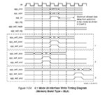
I was thinking i must have made some error while following write timing diagram(given in xilinx manual).

Yeah,i'll try debugging ip-core as well.

Attachment:Write timing diagram as per manual.
 

Attachments

  • Capture.JPG
    Capture.JPG
    72.8 KB · Views: 55

You are aware that the MIG DDR controllers go through a training sequence? Are you waiting for the training sequence to finish and the core reports it's "ready"?
 

Hi,

By training sequence,if you mean calibration(signal init_calib_complete) signal which goes high when you run simulation for 100 us or more depending on your design,yes,i'm waiting for i to go high.

All the above waveforms are after calibration is completed.
 

By training sequence,if you mean calibration(signal init_calib_complete) signal which goes high when you run simulation for 100 us or more depending on your design,yes,i'm waiting for i to go high.

All the above waveforms are after calibration is completed.

That means you'll have to resort to my other suggestion and trace the user side signals into the core to find out why your write transactions aren't getting to the memory.

You did verify that your data does not show up on the interface between the FPGA and your DDR3 memory model?
 

That means you'll have to resort to my other suggestion and trace the user side signals into the core to find out why your write transactions aren't getting to the memory.
Yeah,i'll try that.
You did verify that your data does not show up on the interface between the FPGA and your DDR3 memory model?
Yeah,like app_wdf_data was the write data signal on the user interface side,ddr3_dq_fpga was the write data at the interface & ddr3_dq_sdram was the write signal which writes into my ddr3 model.
I could see that my desired data is coming to user interface side,but that wierd data is coming at ddr3_dq_fpga.
So,yes it does not show up on the interface between the FPGA and your DDR3 memory model

But,my problem is how is the same wierd data coming at interface side everytime,no matter the input
 

Hi,

@ads-ee:
I made a silly mistake.If you refer to the above timing diagram,i was not asserting app_wdf_end at the same time as app_wdf_wren.Now,that i have done it,ddr3_dq_fpga is getting my desired data.

But some problems remain,about which i'll analyze more and post,so i'll keep this thread active.
 

Status
Not open for further replies.

Part and Inventory Search

Welcome to EDABoard.com

Sponsor

Back
Top