Continue to Site

Welcome to EDAboard.com

Welcome to our site! EDAboard.com is an international Electronics Discussion Forum focused on EDA software, circuits, schematics, books, theory, papers, asic, pld, 8051, DSP, Network, RF, Analog Design, PCB, Service Manuals... and a whole lot more! To participate you need to register. Registration is free. Click here to register now.

Eye diagram of specific time interval instead of the whole transient time

Status
Not open for further replies.

henry kissinger

Member level 2
Joined
Nov 19, 2021
Messages
44
Helped
0
Reputation
0
Reaction score
0
Trophy points
6
Activity points
442
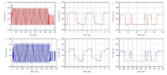
ADS function 'FrontPanel_eye()' can create eye diagram from the transient voltage of a circuit node.

However if I only want the eye diagram at specific interval instead of the whole transient time. How should I do it?

Below graph on the left are the 0~450nsec (whole transient time). I am only interested in 0~10 nsec and over 400 nsec. How should I create eye diagram of these 2 interval?
 

Attachments

  • eye.JPG
    eye.JPG
    110.5 KB · Views: 94

Hi,

I can´t answer your question...

But I wonder if an eye diagram for such a short time makes sense at all.

Klaus
 

My approach is to place a vpulse source set up at the eye interval with tf=1n, pw=1n, tr=cycle-2n and use that as the "local time base" to "rasterize" the waveform into an eye diagram. Changing td= will change the start point and relation to the main clock.

Then plot against v(myVpulse_plus) on the X axis.
 

One can recycle the pattern you wish to test and rely on your stable clock for any choice of bit length or use single shot triggers using the clock and enabled by the data pattern. This can also measure the phase-amplitude margin in other methods. One such method is to delay the clock with linear or adjustable delays for early , PLL nominal and late pulse, then count accurate data in all samples. These delays can also be contributed to data to produce a pseudo-random early-nom-late bit shift then increase the delays until errors occur in one packet or burst or any length of measure.

Normally for clock and data recovery you have a budget for all the effects of amplitude and phase distortion. In logic systems it would be just measured in window margin and before the slicer in eye pattern with margin vs number of bits for a particular pattern.

- In RLL codes the spacing between min/max will have different group delays in the channel that must be designed. This can be minimized with raised cosine channel filters.
- the data slicer will have asymmetry that contributes to margin loss
- The clock stability also has jitter. This can be minimized with PLL compensation filters to suppress random noise, jitter, and offset.
- mismatched impedances will have amplitude echos and ripple such as in your plots. This can be minimized with an active terminator or pull-up/dn resistors to match the channel Zo unless there are excessive stubs in MIMO channel.

- there are asymmetric propagation delays based on asymmetric impedances or push/pull currents and also other root causes. This will show up in different worst-case data patterns. Each RLL code has differ

- Phase margin Analyzers come in all types depending on the bandwidth, bit rate and protocol

Once you have a design budget and verify the design meets the budget then the BER can be controlled vs the bit shift and projected in ps/decade # of bits or the uncorrected or corrected error rate base on the SNR and Window margin..
 

I don't use that tool but the one I do, has functions like
"clip()" that will return a portion of the tran vector to
the calling operation (like plot, or a calculation). If you
want to focus in or exclude startup, etc.
 

Status
Not open for further replies.

Part and Inventory Search

Welcome to EDABoard.com

Sponsor

Back
Top