Continue to Site
Follow along with the video below to see how to install our site as a web app on your home screen.
Note: This feature may not be available in some browsers.
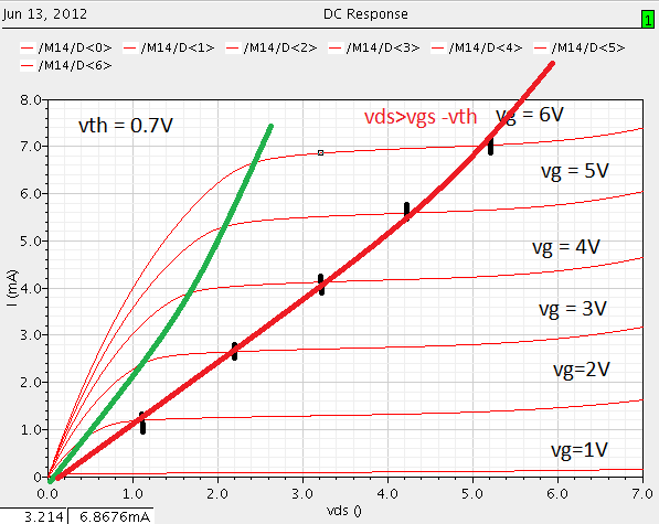
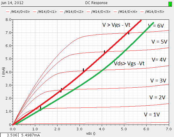
tangent of green gives ON resistance or ESR of 1V/6mA=167 Ω
The Red load line looks like 780Ω so Gm looks better or transconductance value.
Is there a load resistance?
Yes. The transistor enters saturation only at red line points but the region between green and red lines is also considered as Active region or Triode Region of the transistor's operation.
All the best.
I agree with sunny too.
- - - Updated - - -
Yes. Its no load condition only. U got to see its model properties for further details on the transistor's behaviour.
Is the Vth 0.7? The defualt value of Vth in spice model is 0.7, but mostly it wont be 0.7 in high technology node.
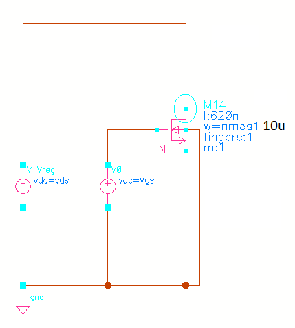
Test bench shown in #3 is not correctly simulated as Drain-Source voltage is not varying with Drain-source resistance. I mean is by this circuit you will see false region shown by red line. MOSFET comes in saturation from green line, because slope is very less shows device reached saturation.
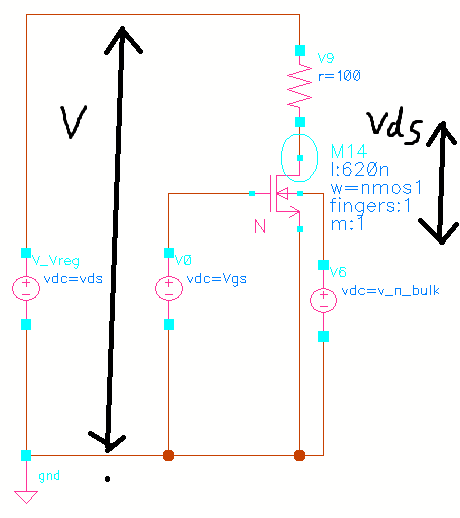
To correct test-bench, add 10k resistance at the drain and then simulate.
First thing you need to know that, before going to test the behavior of device, the device should have been correctly biased.
So now, please make sure, device can carry the biased drain current. If you sweep the supply, MOSFET should not cross break down limits.
Now, please tell us, what is the drain current, what is the device width, and what is the drain-source resistance?
(to limit drain current use the appropriate load resistance)
Reason is, if you bias incorrectly, may be the device model you are using not correct.
Hope you understood my point.
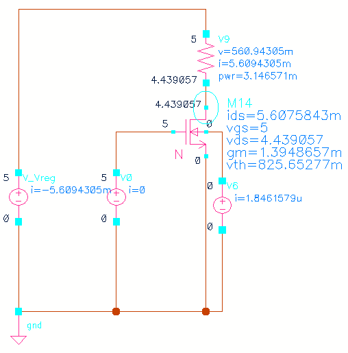
Ah, better you bias it with 10-100uA. and then check the response.
---
by the way, the shown MOSFET is 5V device, right? then it can't withstand 7V. Check the pdk please.
Actually ideal curves as per Vds>Vgs-Vth for saturation will be different from the one which u got.
They will keep increasing till the red line points and will become constant from there on.
Here they seem constant from green line points itself. Its because of varying model properties. A transistor in any model will be defined by some 90 plus properties.
- - - Updated - - -
The region between green line points and red line points is termed as "sub-threshold" region of operation.
It occurs just before entering the saturation region. This concept will be available in many VLSI text books.
Just refer to it.
What is meant by this?It doesn't looks pratical for this testbench......