Continue to Site

Welcome to EDAboard.com

Welcome to our site! EDAboard.com is an international Electronics Discussion Forum focused on EDA software, circuits, schematics, books, theory, papers, asic, pld, 8051, DSP, Network, RF, Analog Design, PCB, Service Manuals... and a whole lot more! To participate you need to register. Registration is free. Click here to register now.

etching: trace width reduction

Status
Not open for further replies.

buenos

Advanced Member level 3
Joined
Oct 24, 2005
Messages
960
Helped
40
Reputation
82
Reaction score
24
Trophy points
1,298
Location
Florida, USA
Activity points
9,116
hi

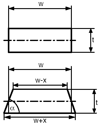
how to calculate trace width reduction caused by etching ?

I have a formula:
W1= W_design - (copperthickness/2)
W2= W1 - (copperthickness/2)

is it correct always? or it depends on the machines used by the manufacturer?

what about the widths on an outer layer?
there the plating makes it to be more difficoult.
 

Hi, I know the formulas are right in ideal conditions.Quality of pcb is depend on machines and method of manufacturing pcb.Pcb manufacturer have different accuracy but a good manufacturer have to follow standards of manufacturing pcb.
 

Your formula is seriouly affected by the actual manufacturing environment of your PCB fabricator. It is very hard to say and give you an universal formula. Generally speaking, in base copper 0.5oz or 1oz case, w1 and w2 won't have a big difference. But it comes to 2oz and 4oz case, there is another story.
 

i have to start with something.
my equations are modelling equations. modelling is never 100% accurate, but much more accurate than nothing. i asked for values from 2 different manufacturers, their values were littlebit different.
i will never use more than 1oz for controlled impedance on my digital boards.
so i still need general formulas.

for outer layer: is it good?
W1= W_design - ((base_copperthickness+copperplating)/2) + 2 * NIAu_plating_thickness
W2= W1 - ((base_copperthickness+copperplating)/2)
 

If you use it to calculate the IMP control, it goes well. But you'd better respect the PCB manufacturer's comment if they need to resize the imp track width to better control impedance. They always can better understand their own manufacturing truth than designers.
Just take a look at 3mil, 10mil and 100mil track width, the situation never go with your formular. Even your design can affect the W1 and W2. Such as many many tracks in a narrow area or only several tracks in a big area, things completely different.
 

i have a bad experience with a manufacturer. about impedance on a given frequency. Er is given on 1MHz by the material manufacturers, but in a real design obviously not all the signals are 1MHz. This manufacturer just didnt care about is. example: 60 ohm traces signal highest freq is 1.2GHz. To use an impedance control software (polar) with Er given on 1MHz i had to pre-distort the impedance, so i have calculated trace width with 58.7 ohm @1MHz to get 60 ohm @1.2GHz. they thought that I my calculation was wrong for 60 ohms because of this... Sometimes they have some not skilled empélloyees who dont know these etching parameters and they cant even use their on impedance software correctly. once my contact guy went to holyday, and the substituter guy made these mistakes.
after this, I dont trust in manufacturers in impedance control anymore.

Added after 5 minutes:

"many many tracks in a narrow area or only several tracks in a big area, things completely different. "
thats why we need copepr balancing, or thieving, to make things to be not different
 

I still remember the dialogue with our process engineer, Er won't be changed very much in the case of 1MHz or 1GHz in fact. You see, 58.7 ohm @1MHz = 60 ohm @1.2GHz. But as far as I know, the general imp tolerance in most factories are 10%. The difference 1.3ohm should be covered by the manufacturing tolerance in most cases and won't affect your case very much. Not sure it is ok to you.
 

With usual fine line PCB technology (w=75..100 um), I expect w1 = w, which comes true in most cases. Most of my fast signal designs have a designed trace impedances which would be hopefully met by e. g. +/- 20 %. Controlled impedance in contrast would imply test structures on the board respectively the production panel and an explicite impedance specification for this structures that has to be checked by the PCB manufacturer.
 

one manufacturer told me these data:
W_design=100um --> w1=90um w2=80um with inner layer copper thickness of 17um.

if the tolerance is 15% then i think the 2.1% (1.3ohm) would not be within the 15% but it would increase it to 17.5%. i think calculation (field solver like polar software) should be within 0.5% then teh production tolerance should be within 15%, but if you manufacture 1000 boards, the average impedance of all boards should be nominal+/-zero, with gaussian distribution.

Added after 2 minutes:

oh, and when they check the impedance, i am shure that at least few of them use the same signal rise time for all boards, all traces, which is incorrect. because they should use the rise times for each signal-trace separatelly given by the hardware design engineer.
 

Your back-etching calculation is apparently based on the assumption, that a PCB manufacturer would plot the gerber data as-is. Usually, he applies a correction to apertures. Here is an example how a manufacturer sees the relation between nominal and actual trace geometry:

28_1208701462.gif


The other point is, that you can't expect impedance tolerances of a few ohms without impedance controlled PCB production, that means, the manufacturer knows the impedance specification of a defined test structure and adjusts his process parameters.
 

"that a PCB manufacturer would plot the gerber data as-is."
if we tell them not to do impedance control on this board, then they will not. what i described above: i made impedance control on a board, then they wanted as well, they sent me their results and those were less accurate than mine.
they measured by TDR (probably with incorrect rise times, but even then), and these were the results on my 60ohm@1.2GHz traces:

Code:
REQUIREMENT				  MEASUREMENT	
NOMINAL	TOLERANCE		MINIMUM	MAXIMUM
58	10%						60	61

they say my requirement was 58?????? it was 60@1.2GHz, which is 58.7@1MHz. ad with a TDR probably they setted up a sort rise time: 30ps...600ps where 410ps would be my signal rise time. from my trace widths they have calculated back the 58 ohms. do i have to explain more?

Added after 5 minutes:

so everyone says i shouldnt care about it, let the pcb fab to do that.

i know how to let them to do that, but i dont know how to make the equations. my question was about this.

it doesnt mean that then i will give up. i know most of the designers let the fab to do that, but i dont care. what i care about is the equations.
 

Status
Not open for further replies.

Part and Inventory Search

Welcome to EDABoard.com

Sponsor

Back
Top