Continue to Site

Welcome to EDAboard.com

Welcome to our site! EDAboard.com is an international Electronics Discussion Forum focused on EDA software, circuits, schematics, books, theory, papers, asic, pld, 8051, DSP, Network, RF, Analog Design, PCB, Service Manuals... and a whole lot more! To participate you need to register. Registration is free. Click here to register now.

ESD Protection and GND_EARTH

Status
Not open for further replies.

ctzof

Full Member level 3
Joined
Mar 1, 2012
Messages
157
Helped
12
Reputation
24
Reaction score
11
Trophy points
1,298
Location
Munich
Activity points
2,516
Hallo,

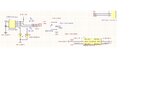
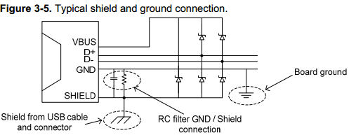
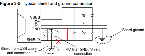
I want to create an esd protection for my USB port. Searching on the internet I've found many possible configurations so I decided to use the following. I've created a GND_EARTH plane where USB Shield is connected. This plane is connected to the normal GND through an RC filter. ESD diodes are connected to each USB signal to GND_EARTH. For the data lines I use STF203 which is also connected to GND_EARTH and VBUS (5V) from USB. GND_USB is connected to normal GND directly. The thing is I'm not really sure if this configuration is correct and won't create any problem due to different grounds in the circuit. Attached you can find a picture of the circuit.
 

Attachments

  • USB.jpg
    USB.jpg
    122.9 KB · Views: 407

i'd say caps or diodes to the earth ground sounds like the best protection , yes
 

The thing is I'm not really sure if this configuration is correct and won't create any problem due to different grounds in the circuit. Attached you can find a picture of the circuit.
Your doubts are substantiated. The configuration isn't correct, particularly connecting the TVS array to GND_EARTH (USB shield). Use the standard configuration suggested by the TVS manufacturer, don't reinvent the square wheel.
 

Your doubts are substantiated. The configuration isn't correct, particularly connecting the TVS array to GND_EARTH (USB shield). Use the standard configuration suggested by the TVS manufacturer, don't reinvent the square wheel.

I am not trying to reinvent something. This is a common method suggested by many. For example Atmel (https://electronics.stackexchange.com/questions/151015/emi-esd-protection-for-usb-interface) I am not sure about the STF203 chip which is tvs and esd filter at the same package.
 

Hi ctzof,

Pcb layout, gnd loop have significant effect on esd performance. Generally, the shunt diodes should place close to USB connector so that the pulses will divert to gnd without getting into the system.
 

Hi ctzof,

Pcb layout, gnd loop have significant effect on esd performance. Generally, the shunt diodes should place close to USB connector so that the pulses will divert to gnd without getting into the system.

Thanks for the answer. I understand that esd diodes should be placed as close as possible to the connector. The question is if there is a problem to be connected to GND_EARTH.
 

I believe that's rather a sketching fault than intentionally designed. In any case it's completely wrong.


- - - Updated - - -

Should be:


I believe that's rather a sketching fault than intentionally designed. In any case it's completely wrong.

Should be:


I agree completely with this drawing. The data lines were unprotected in the other drawing. This is the way to go.
 

I was a high voltage spark generator for one winter.
I bought some high quality Name Brand shoes that used synthetic leather for the soles so they have long tread life. When the humidity was low and I walked on a carpet I generated a whopping high voltage arc when I got near an electrical device that was grounded. I caused the telephone system at work to reset whenever I got near it. I needed to be careful with ESD when I worked with Cmos circuits.

Some carpets have very fine wires woven in them that are grounded to prevent ESD.


The USB specification says that the connector shield should be connected to device chassis but doesn't prescribe a grounding method. However you connect the USB shield to GND, it should be clear that ESD surges must be primarly clamped relative to signal ground to avoid damage of the interface components.
 

I was a high voltage spark generator for one winter.
I bought some high quality Name Brand shoes that used synthetic leather for the soles so they have long tread life. When the humidity was low and I walked on a carpet I generated a whopping high voltage arc when I got near an electrical device that was grounded. I caused the telephone system at work to reset whenever I got near it. I needed to be careful with ESD when I worked with Cmos circuits.

One thing you could do is make your self a grounding touch pad that you discharge before grounding your self to wrist strap and earth ground. The touch pad could be a small square of copper that attaches to the earth ground through a 10 MegOhm resistor.
 

Its difficult to answer weather this configuration is right or wrong. By the way I made one of these boards with this configuration and seem to work. I just have to check if they are protected from esd transients.
 

Status
Not open for further replies.

Similar threads

Part and Inventory Search

Welcome to EDABoard.com

Sponsor

Back
Top