Welcome to our site! EDAboard.com is an international Electronics Discussion Forum focused on EDA software, circuits, schematics, books, theory, papers, asic, pld, 8051, DSP, Network, RF, Analog Design, PCB, Service Manuals... and a whole lot more! To participate you need to register. Registration is free. Click here to register now.
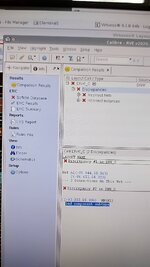
I would like to ask help regarding this error from the layout.
I using TSMC 0.18um 1P6M process.
My design requires an NMOS with a shorted source and bulk.
I would like to ask help regarding this error from the layout.
I using TSMC 0.18um 1P6M process.
My design requires an NMOS with a shorted source and bulk.
If you put NMOS in a DNW/VNW pocket then its body is cut
off from the bulk / handle Psub and you will have to route the
body (tap) explicitly to open field and a ptap there.
What value do you imagine putting it in a DNW pocket is,
when you intend to jumper it to the substrate in the end?
You eat a lot of layout area for nothing (except perhaps
substrate noise control).
So then you do not want source tied to "bulk" (which is the
handle Psub / Pepi) but the local body "pocket" (Pepi inside
DNW/VNW). That may want you to use a 4T FET symbol and
wire it explicitly; the 3T may have an inherited sub! connection
that you either can't modify or can't find?
This site uses cookies to help personalise content, tailor your experience and to keep you logged in if you register.
By continuing to use this site, you are consenting to our use of cookies.