Continue to Site

Welcome to EDAboard.com

Welcome to our site! EDAboard.com is an international Electronics Discussion Forum focused on EDA software, circuits, schematics, books, theory, papers, asic, pld, 8051, DSP, Network, RF, Analog Design, PCB, Service Manuals... and a whole lot more! To participate you need to register. Registration is free. Click here to register now.

EMI/EMC test getting failed @30-60MHZ in Radiated emission

Status
Not open for further replies.

svg

Member level 1
Member level 1
Joined
Feb 18, 2013
Messages
39
Helped
0
Reputation
0
Reaction score
0
Trophy points
1,286
Visit site
Activity points
1,547
Hi All,

our product is very similar to TABLET.last week we gone for EMI/EMC test.product got passed in Conductive Emission but failed in RE @ 40-60MHZ. our circuit has one dc-dc switcher with step up transformer for generating 200v power.

Please provide me suggestion to pass in EMI test.I want to remove that peak emission.is there any filter/snubber/any other option to remove that spike? If you have any doubt,Please let me know.
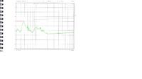
 

I think the problematic range of frequency is from 33MHz to 65MHz. It will be better if you share the schematics of your circuit to suggest you proper solution.

Review this ferrite bead BLM15PX601SN1 - this may help reduce the emissions in the said frequency range.
 
  • Like
Reactions: svg

    svg

    Points: 2
    Helpful Answer Positive Rating
Thank you for your reply!!!

Where we can put the ferrite bead? input/output side.
Already we put 10uF(4 nos) at input to that transformer. we tried of putting shield over the transformer,but nothing helped.
 

The ferrite bead has to placed at the output from the switcher so that the switcher harmonics will be suppressed before they couple to other parts of the circuit or get radiated.

But in any case it will be good if you share at least the partial schematics so that the members here can provide you with useful tips.
 
  • Like
Reactions: svg

    svg

    Points: 2
    Helpful Answer Positive Rating
I will sent you the schematic shortly.
is there any other way to sort out the problem? other than ferrite bead.
 

Are you aware of the switching or other frequencies on your board? If you know the frequencies on your board, you can inspect which section(s) may cause the radiation. According to the given spectrum, the problematic frequency is 48 MHz. Is there a block operating around 48 MHz, there may also be blocks operating around 16 MHz causing the problem with their 3rd harmonic, even lower frequencies may cause the problem with their higher order harmonics.

Try to determine the offending block and think about how to solve. You can cover them with a shielding. You may use cupper tapes or small shaped shielding covers
 
  • Like
Reactions: angy and svg

    svg

    Points: 2
    Helpful Answer Positive Rating

    angy

    Points: 2
    Helpful Answer Positive Rating
Maybe adjust gate resistor values on the switching power device?
Increase value to reduce switching rise time. This will reduce radiated harmonics.
 
  • Like
Reactions: svg

    svg

    Points: 2
    Helpful Answer Positive Rating
A ferrite bead is more suitable for suppressing conducted emissions, not radiation. For radiated emissions, a picture of the whole thing would be very helpful, especially something showing the transformer construction.
 
  • Like
Reactions: svg

    svg

    Points: 2
    Helpful Answer Positive Rating
I do not see the maximum emission level permitted drawn on the jpg in the original post. Were can i get this information from.
 

yes you are correct. we have sdcard section which is operating at 48Mhz.what we can do for that? any solution?

already we tried of using copper shield over transformer,but no use of that shield.that dc-dc operating at 150khz. we thought that DC-DC switcher is causing the problem.thats why we put shield over transformer. if SD card is making the problem means,what else we can do?? please suggest.......

- - - Updated - - -

refer the image that will give you how schematic looks...


Are you sure that during the RE measurements the SD card functionality was being tested? If it was disabled, then there may be something else which need to be looked into.
 
  • Like
Reactions: svg

    svg

    Points: 2
    Helpful Answer Positive Rating
A snubber on the diode in your switcher may be the answer, even just 100pF (500V) and 47 ohm 400mW, a scope will help you trim the R to get minimum ringing here...
 
  • Like
Reactions: svg

    svg

    Points: 2
    Helpful Answer Positive Rating
Is it possible to disable the SD card section in a way, hard or soft? Try to disable the suspicious section and make sure whether it causes or not. If the problem is that section, focus more to solve. As suggested in previous posts, placing appropriate resistors in traces which are supposed to radiate may reduce the radiaiton without disturbing the function. Shileds, small absorbers may also help to block/absorb the radiation.
 
  • Like
Reactions: svg

    svg

    Points: 2
    Helpful Answer Positive Rating
No we can't disable sd card section and test.because we boot the device using sdcard. without sdcard there is no option for our device to boot.

One more points to be noted,high voltage generation circuit(nearly 200v from 5V) has transformer and high switching MOSFET. is anybody know how to design snubber circuit? answering this question might help us.
 

  • Like
Reactions: svg

    svg

    Points: 2
    Helpful Answer Positive Rating
Status
Not open for further replies.

Similar threads

Part and Inventory Search

Welcome to EDABoard.com

Sponsor

Back
Top