ab_basu
Newbie level 5
Hi,
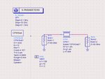
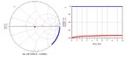
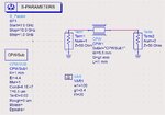
I am new to simulation in ADS, and I want to do EM simulation of a basic CPW structure. I need a step-by-step guide to do so. I used line calculation to optimize Lwisth and length. I have attached the circuit and basic S-parameter of the design (Fig. 1 and 2). Then I generate a layout, that came like Fig. 3. What to do after this? I tried to use substrate as a Si substrate with 1 mm thickness. But I think I am doing something wrong. Please I need it urgently. Somebody, please help.
I am new to simulation in ADS, and I want to do EM simulation of a basic CPW structure. I need a step-by-step guide to do so. I used line calculation to optimize Lwisth and length. I have attached the circuit and basic S-parameter of the design (Fig. 1 and 2). Then I generate a layout, that came like Fig. 3. What to do after this? I tried to use substrate as a Si substrate with 1 mm thickness. But I think I am doing something wrong. Please I need it urgently. Somebody, please help.