Continue to Site

Welcome to EDAboard.com

Welcome to our site! EDAboard.com is an international Electronics Discussion Forum focused on EDA software, circuits, schematics, books, theory, papers, asic, pld, 8051, DSP, Network, RF, Analog Design, PCB, Service Manuals... and a whole lot more! To participate you need to register. Registration is free. Click here to register now.

Electronic Load - conception and transistor choice.

Status
Not open for further replies.

carpenter

Full Member level 6
Joined
Jul 25, 2012
Messages
353
Helped
22
Reputation
44
Reaction score
24
Trophy points
1,298
Activity points
4,467
I need multichannel (4x) electronics load and thinking about simple conceps.

I want what a simple concept, my idea see pic.

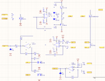
One big N-mosfet + current shunt, one difference amplifier U1B for amplifies voltage from current on shunt, output drive U1A and ADC in any ARM-CortexM3
Voltage in measure second difference amplifier U2B , output drive ADC in any ARM-CortexM3.
ARM-CortexM3 over 1MSPS DAC drive U1A, in CC mode load drive in full analog controll loop , in CV and CR in controll loop is digital over DAC output.
It's a big nonsense?

2 Choice of transistor
need load to 100V, 250W on chanell I search high power MOSFET, I find FDA50N50 500V 105mOhm 625W
Secon choice will be any in SOT-227 , I thing big case better heat dissipation over heatsink,
IXFN55N50 here was why have IXFX IGBT schematics mark?
or IXKN75N60C
600V 75A 36mOhm, unfortunately datasheet is quite auspicious austere .

My question
How much is the SOT227 case more suitable than TO-3PN?
XKN75N60C if big silicon and have big capacitnce , how big the problem it is with a given method of control and use?

**broken link removed**
 

250W can possibly work with a single SOT-227 transistor, if you have a large heatsink with forced cooling. The control circuit needs loop compensation and a series resistor to isolate the gate capacitance. SImilar current source circuits have been discussed quite often at Edaboard. For moderate bandwidth, the OP can drive the gate without booster circuit.
 

Think about things like dynamic response and load mode.
Do you want to impose a current value or a resistance
value? Does the load need to operate symmetrically
about ground (negative as well as positive) and be
linear-ish, as a RF or analog test subject might require?
General purpose, like, or just "get it done over limited
range that suits this project"?

I have built binary weighted, resistor-on-MOSFET gang
loads which can be set to hold a fixed(-ish) resistance
over the FET breakdown range, but this is unidirectional,
granular and still has a wee bit of stray C.

I have had trouble with "active E-loads" (Agilent boxes)
in power supply testing, their response time adds another
frequency-response "mystery element" to loop stability.

A MOSFET load will have a MOSFET I-V characteristic in-the-
moment, until control loop can intervene, so there can
be peculiar edge behaviors on step-load or step-source
events until settling gets done.
 

Ok here is the first draft.,

AS Load is used Mosfet IXFN100N50Q3 RdsOn 49mOhm and in China price under 10$ + 10m Ohm Shunt 10W (in real 50W from china)
Current on MOSFET is measured over U1B difference amplifier with A=5.5 for 30A on 10m Ohm is output voltage 1,65V in secon stage is amplifier U1A with G=2, G=5.3, G=14.1, G=17,4
this output go on ADC in MCU and on -input error Amplifier u2a.
On + input U2A go 0-3,3V from DAC, this error amplifier drive over MOSFET driver Q1+Q4 big MOSFET

Voltage on +- input of load is measured over differnece amplifier U2B witg G= 1/30,3 for 100V is output 3,3V on ADC MCU


In CC mode is current set over DAC_I
In CV mode is Voltage set over DAC_U (second dac in MCU) and this voltge is on internel comparator of MCU compared with ADC_U and comparator drive error amplifiier over Q3
In CR mode wil be make full digital control wher MCU measure ADC_I + ADC_U and drive DAC_I for DAC_I= ADC_U / R.

If use stm32f373 we have
- 2x 1MSPS 12bit DAC 0-3,3V
- 1x High speed 12bit ADC 0-3,3V
- 3x Low speed 16bit ADC
- 2x High speed comparator

If use isolated +12V -12V and 3.3V + isolated USART we have simple and I thing well designed load 0-100V 0-30A max power disipation what I can do to cool down.
In datasheet of IXFN100N50Q3 is max Pd for impulse 960W. The continuous load will depend on the cooler quality and size.

What do you think about it?

ELoad.png
 

Status
Not open for further replies.

Similar threads

Part and Inventory Search

Welcome to EDABoard.com

Sponsor

Back
Top