Continue to Site

Welcome to EDAboard.com

Welcome to our site! EDAboard.com is an international Electronics Discussion Forum focused on EDA software, circuits, schematics, books, theory, papers, asic, pld, 8051, DSP, Network, RF, Analog Design, PCB, Service Manuals... and a whole lot more! To participate you need to register. Registration is free. Click here to register now.

EFR32FG14 SPI Chip Select problem

Status
Not open for further replies.

yefj

Advanced Member level 4
Joined
Sep 12, 2019
Messages
1,188
Helped
1
Reputation
2
Reaction score
3
Trophy points
38
Activity points
7,167
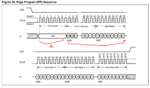
Hello,I am trying to communincate using SPI protocol and send the pattern bellow with manual rise of Chip Select between every command of the 6 commands.

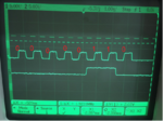
As you can see bellow i managed to send all six bytes at once as you can see bellow.

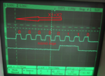
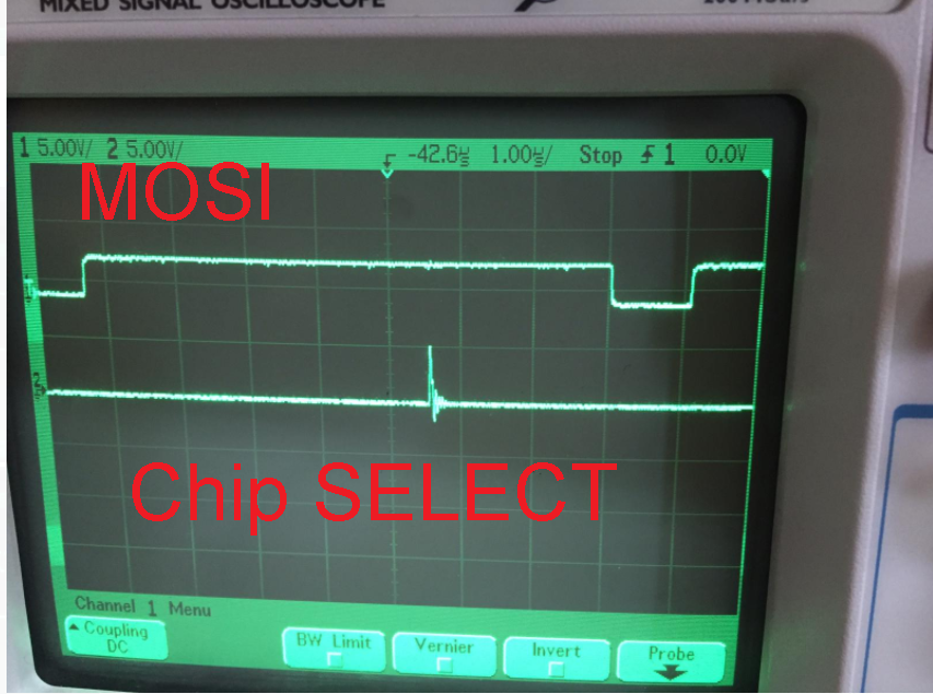
I was imagining to see the CS Rise between them with the same width of 1 bit as in the MOSI pattern .

But in reality i get CS jump with some glitch like pattern, and they are not between the commands

The full code is attached bellow.


Where did i go wrong implementing the manual Chip select?

Thanks.


1599054183650.png


Code:
/**************************************************************************//**
* @main_series1_PG1_EFR.c
* @brief Demonstrates USART1 as SPI master.
* @version 0.0.2
******************************************************************************
* @section License
* <b>Copyright 2018 Silicon Labs, Inc. http://www.silabs.com</b>
*******************************************************************************
*
* This file is licensed under the Silabs License Agreement. See the file
* "Silabs_License_Agreement.txt" for details. Before using this software for
* any purpose, you must agree to the terms of that agreement.
*
******************************************************************************/

#include "em_device.h"
#include "em_chip.h"
#include "em_cmu.h"
#include "em_gpio.h"
#include "em_usart.h"
#include "em_ldma.h"

#define TX_WREN_BUFFER_SIZE   1
#define TX_WRSR_BUFFER_SIZE   4
#define TX_RDSR_BUFFER_SIZE   1

#define RX_BUFFER_SIZE   1


uint8_t Tx_WREN[TX_WREN_BUFFER_SIZE] = {0x06};//write enable command
uint8_t Tx_WRSR[TX_WRSR_BUFFER_SIZE] = {0x01,0x2F,0xEF,0xD8}; //write status register
uint8_t Tx_RDSR[TX_RDSR_BUFFER_SIZE] = {0x05}; //read status register

uint32_t TxBufferIndex = 0;

uint32_t RxBuffer;
//uint32_t RxBufferIndex = 0;

volatile uint32_t msTicks; /* counts 1ms timeTicks */

void Delay(uint32_t dlyTicks);
void SysTick_Handler(void)
{
  msTicks++;       /* increment counter necessary in Delay()*/
}
void Delay(uint32_t dlyTicks)
{
  uint32_t curTicks;

  curTicks = msTicks;
  while ((msTicks - curTicks) < dlyTicks) ;
}


int main(void)
{
     CHIP_Init();
    CMU_ClockEnable(cmuClock_GPIO, true);
        CMU_ClockEnable(cmuClock_USART1, true);
        CMU_ClockEnable(cmuClock_USART0, true);

        // Configure GPIO mode
        GPIO_PinModeSet(gpioPortC, 8, gpioModePushPull, 0); // US1_CLK is push pull
        GPIO_PinModeSet(gpioPortA, 4, gpioModePushPull, 1); // US1_CS is push pull
        GPIO_PinModeSet(gpioPortC, 6, gpioModePushPull, 1); // US1_TX (MOSI) is push pull
        GPIO_PinModeSet(gpioPortC, 7, gpioModeInput, 1);    // US1_RX (MISO) is input

        // Start with default config, then modify as necessary
        USART_InitSync_TypeDef config = USART_INITSYNC_DEFAULT;
        config.master       = true;            // master mode
        config.baudrate     = 1000000;         // CLK freq is 1 MHz
        config.autoCsEnable = false;            // CS pin controlled by firmware, not hardware
        config.clockMode    = usartClockMode0; // clock idle low, sample on rising/first edge
        config.msbf         = true;            // send MSB first
        config.enable       = usartDisable;    // Make sure to keep USART disabled until it's all set up
        USART_InitSync(USART1, &config);

        USART_InitAsync_TypeDef init = USART_INITASYNC_DEFAULT;

        // set pin modes for UART TX and RX pins
          GPIO_PinModeSet(gpioPortA, 1, gpioModeInput, 1);
          GPIO_PinModeSet(gpioPortA, 0, gpioModePushPull, 1);
          ///////////////////////////////////

            USART_InitAsync(USART0, &init);

            USART0->ROUTELOC0 =(USART_ROUTELOC0_TXLOC_LOC0)  | // US1_TX (MOSI) on location 11 = PC6 per datasheet section 6.4 = EXP Header pin 4
           (USART_ROUTELOC0_RXLOC_LOC0);   // US1_RX (MISO) on location 11 = PC7 per datasheet section 6.4 = EXP Header pin 6

        // Set USART pin locations
        USART1->ROUTELOC0 = (USART_ROUTELOC0_CLKLOC_LOC11) | // US1_CLK       on location 11 = PC8
                            (USART_ROUTELOC0_CSLOC_LOC11)  | // US1_CS        Manual
                            (USART_ROUTELOC0_TXLOC_LOC11)  | // US1_TX (MOSI) on location 11 = PC6
                            (USART_ROUTELOC0_RXLOC_LOC11);   // US1_RX (MISO) on location 11 = PC7

        // Enable USART pins
        USART1->ROUTEPEN = USART_ROUTEPEN_CLKPEN  | USART_ROUTEPEN_TXPEN | USART_ROUTEPEN_RXPEN;
        // Enable USART1
           USART_Enable(USART1, usartEnable);
           TxBufferIndex = 0;
           while(1)
     {
              // Write enable command
               GPIO_PinOutClear(gpioPortA,4);
               USART_Tx(USART1, Tx_WREN[0]);
                GPIO_PinOutSet(gpioPortA,4);

                GPIO_PinOutClear(gpioPortA,4);
             USART_Tx(USART1, Tx_WRSR[0]);
             USART_Tx(USART1, Tx_WRSR[1]);
             USART_Tx(USART1, Tx_WRSR[2]);
             USART_Tx(USART1, Tx_WRSR[3]);
               GPIO_PinOutSet(gpioPortA,4);

               GPIO_PinOutClear(gpioPortA,4);
                 USART_Tx(USART1, Tx_RDSR[0]);
               RxBuffer = USART_Rx(USART1);
                 GPIO_PinOutSet(gpioPortA,4);


                 //    USART_Tx(USART0,RxBuffer);

                 //    USART_Tx(USART0, '\n');
             }

}
 
Last edited:
Hi,

The device does exactly what the code says.

It sets CS .... no wait ... then it clears CS.
--> add some delay between set and clear.

mind: it is manually controlled, thus it has nothing to do with SPI clock.

Klaus
 
Hello Klauss ,How do i shut down the clock signal when my manual CS goes high?
another question Is I cant find in the manual shown bellow the rules for the Chip select Like What is the minimal amount of time high CS is required in order for it to understand that the command tranfser completed?
How many bits we can sendat most in a single Chips select Low session ?
Thanks.

Thanks.
Hi,

The device does exactly what the code says.

It sets CS .... no wait ... then it clears CS.
--> add some delay between set and clear.

mind: it is manually controlled, thus it has nothing to do with SPI clock.

Klaus
 
Last edited:

Hi,

Clock usually is just (8 times) active when you send a byte. When you don't send a byte, then clk is idle. Independent of CS.

CS timing.
The chip uses a SYNC signal instead of a SPI standard CS signal. It seems it is designed to be compatible with a CS signal.
However, the timing is clearly specified in "7.6 DACx0004 Timing Requirements".

And it also says:
8.4.1.2.1 SYNC Interrupt – Daisy-Chain Mode
For daisy-chain operation, the SYNC line stays low for at least 32 × N SCLK cycles, where N is the number of
DACx0004s in the daisy chain. If SYNC is brought high before a multiple 32 SCLKs, it acts as an interrupt to the
write sequence;


Klaus
 

I found https://www.silabs.com/documents/public/reference-manuals/efr32xg14-rm.pdf and Section 18.3.3 seems to clearly show how the SPI mode works.
18.3.3.3 says that the clock is only active while there are values to exchange - which is the normal way things work.
18.3.3.4 shows how the \CS\ pin works in the various modes. You have it set up to be manual which means that it will lowered and raised in your code when you say it will be.
Looking at your code, you seem to assume that the USART_Tx function will bock until the value exchange has completed. You need to check that this is the case - and if it isn't (in other words that it simply queues up the value in the USART hardware buffer if there is room) then you need to detect when the buffer is empty and raise the \CS\ pin.(That USART seems to have the ability for the hardware to control the \CS\ line while the buffer is not empty. However you then need to make sure that the buffer is empty BEFORE you start queuing up new values to exchange - there is no free lunch!)
Susan
 
  • Like
Reactions: yefj

    yefj

    Points: 2
    Helpful Answer Positive Rating
Hello Aussie Susan, We have the follwing command
Code:
USART_Tx(USART1, Tx_WRSR[0]);
You say i should check the USART1 hardware buffer is empty and ready to send abother frame.
We could use the following line which will run until TXBL is 1.
TXBL is an interrupt so i think i should use to check if i can send data
Code:
USART1->IEN = USART_IEN_TXDATAV;

Code:
while( !(USART1->STATUS & (1 << 6)) );
We could also empy both transmit buffer and Tx shift register
Code:
USART1->CMD |= (1 << 10)
SO How should i incorporate those three elements together,I put the clear command and wait till TXBL=1 between each send command?
Is The code shown bellow implements the Issue you mentioned?
Thanks
Code:
USART1->IEN = USART_IEN_TXDATAV;


GPIO_PinOutClear(gpioPortA,4);
             USART_Tx(USART1, Tx_WRSR[0]);
while( !(USART1->STATUS & (1 << 6)) );
USART1->CMD |= (1 << 10)

             USART_Tx(USART1, Tx_WRSR[1]);

while( !(USART1->STATUS & (1 << 6)) );
USART1->CMD |= (1 << 10)
             USART_Tx(USART1, Tx_WRSR[2]);
while( !(USART1->STATUS & (1 << 6)) );
USART1->CMD |= (1 << 10)
             USART_Tx(USART1, Tx_WRSR[3]);
               GPIO_PinOutSet(gpioPortA,4);


1599123406012.png


Looking at your code, you seem to assume that the USART_Tx function will bock until the value exchange has completed. You need to check that this is the case - and if it isn't (in other words that it simply queues up the value in the USART hardware buffer if there is room) then you need to detect when the buffer is empty and raise the \CS\ pin.(That USART seems to have the ability for the hardware to control the \CS\ line while the buffer is not empty. However you then need to make sure that the buffer is empty BEFORE you start queuing up new values to exchange - there is no free lunch!)
Susan
 
Last edited:

Hi,

clearing the TX buffer will stop data transmission and thus the data transfer will not be complete. --> Communication error.
So this is not an option.

You need to read the library´s documentation whether the send_UART is blocking or not.
If there is a blocking function, then use it.
If there is no blocking function you need to read the UART status and wait until transfer is finished.

Klaus
 
  • Like
Reactions: yefj

    yefj

    Points: 2
    Helpful Answer Positive Rating
Hello Klauss ,USART_tx is not blocking.There is SPIDRV command which is blocking but it does not work with manual Chip select.
So the alogrithm for block as i think it should be,is as following:
Clearing transmit buffer and Tx shift register->transmitting[0]->waiting->trinsmiting[1]->etc..->CS_high with half second delay.
As shown in the code bellow.
is that the blocking mechnism you suggested?
Thanks.
Code:
USART1->IEN = USART_IEN_TXDATAV; //enable TXBL interrupt flag

USART1->CMD |= (1 << 10)  //To clear junk data  from transmit buffer and Tx shift register
GPIO_PinOutClear(gpioPortA,4); //Low CS


USART_Tx(USART1, Tx_WRSR[0]);//transmit first byte of the command

while( !(USART1->STATUS & (1 << 6)) );  //wait TILL TXBL goes high

USART_Tx(USART1, Tx_WRSR[1]);//transmit second byte of the command

while( !(USART1->STATUS & (1 << 6)) );  //wait TILL TXBL goes high

USART_Tx(USART1, Tx_WRSR[2]);//transmit third byte of the command

while( !(USART1->STATUS & (1 << 6)) );  //wait TILL TXBL goes high

USART_Tx(USART1, Tx_WRSR[3]);//transmit 4th byte of the command

while( !(USART1->STATUS & (1 << 6)) );  //wait TILL TXBL goes high

GPIO_PinOutSet(gpioPortA,4); //High CS so signal the end of SPI session

delay(500) //delay half a second so the device will understand that trnasmition is OVER
 
Last edited:

Hi
Hello Klauss ,USART_tx is not blocking.There is SPIDRV command which is blocking but it does not work with manual Chip select.
So the alogrithm for block as i think it should be,is as following:
Clearing buffer->transmitting[0]->waiting->trinsmiting[1]->etc..->CS_high with half second delay.
As shown in the code bellow.
is that the blocking mechnism you suggested?
Thanks.
You urgently need to read documentation.
All libraries I know have at least one blocking UART_send function. Check if it exists. This is the most simple solution.

****
alternative solution:
(no time delay)
just check the UART_busy flag in a loop until cleared.

****
Why don´t you want the automatic CS control? Why the effort for manual control?

Klaus
 
  • Like
Reactions: yefj

    yefj

    Points: 2
    Helpful Answer Positive Rating
Because my USART1 sync is all port E whereas the CS is port A pin4 for some reason.
this is how my hardware is connected, so i need to do manual CS because no usart location has both port E and port Apint 4 CS.
What do you think about the clearing command in the start ,is it ok to clear all for a fresh start of the sending session?
Thanks.
USART1->CMD |= (1 << 10) //To clear junk data from transmit buffer and Tx shift register


Why don´t you want the automatic CS control? Why the effort for manual control?
 
Last edited:

Hi,

why do you expect something to be in the buffer?

SPI does not wait for an event, it sends out data as soon as you start.
And I don´t recommend to stop any transfer... it just causes errors and/or confusion. Thus there should be no data left in the Tx buffer.

Klaus
 
  • Like
Reactions: yefj

    yefj

    Points: 2
    Helpful Answer Positive Rating
Hello Klauss, i am trying to do in parralel SPI with MX25 with the manual link shown bellow.
I have tried to look for timing requirements and i found the photo bellow in the manual.
But i cant see what is the maximal amount of bytes i can send in a single Chip select low session.
If you could please help me with this issue.
Thanks.


**broken link removed**
1599141169537.png

Hi,

Clock usually is just (8 times) active when you send a byte. When you don't send a byte, then clk is idle. Independent of CS.

CS timing.
The chip uses a SYNC signal instead of a SPI standard CS signal. It seems it is designed to be compatible with a CS signal.
However, the timing is clearly specified in "7.6 DACx0004 Timing Requirements".

And it also says:
8.4.1.2.1 SYNC Interrupt – Daisy-Chain Mode
For daisy-chain operation, the SYNC line stays low for at least 32 × N SCLK cycles, where N is the number of
DACx0004s in the daisy chain. If SYNC is brought high before a multiple 32 SCLKs, it acts as an interrupt to the
write sequence;


Klaus
 
Last edited:

Hi,

now a different chip...
Are you confused? At least I am....

What do you mean by "parallel SPI" ? SPI is serial...

byte count in READ:
Datasheet says at 10-11:
The address is automatically increased to the next higher address after each byte data is shifted out, so the whole memory can
be read out at a single READ instruction. The address counter rolls over to 0 when the highest address has been reached.

also see the other READ chapters.

byte count in WRITE:
read section 10-23
see figure 30

Klaus
 

Hello Klauss, I Want to Write data to this device and read from it.
For writing At first i though i should do those two commands
1st command {0x06};//write enable command
2nd command {0x01,0x2F,0xEF,0xD8}; //write status register based on the table bellow
But then with your help i saw The PP command which from FiG30 shown bellow which starts with 0x02.
So I assume that in order to Store data on this device i need to add 0x02 to my sequence as following:(send MSB first )

1st command {0x06};//write enable command
2nd command {0x02,0x01,0x2F,0xEF,0xD8} PP sequence and Write STATUS register the data 0x2F,0xEF,0xD8.
did i assembled the sequence correctly for this command?
THanks.

**broken link removed**

1599158521151.png

1599155770302.png
 

Attachments

  • 1599155686090.png
    1599155686090.png
    156.3 KB · Views: 96

Hi,

If I'm not mistaken then there is a complete flow chart for writing data in the datasheet.
Please take the time and read the datasheet.

Klaus
 
Hello Klauss, So if understand correctly for example i want to write to adress all zeros the value of 1111 1111 which is FF in hex so the correct command is
0x02,0x00,0x00,0x00,0x00,FF
So first the {0x06};//write enable command in the start?
then the PP command 0x06,0x02,0x00,0x00,0x00,0x00,FF
If i want to read from that adress the value FF then i should do by fig18 to do
0x03,0x00,0x00,0x00,0x00
correct?
**broken link removed**
1599223324750.png
 
Last edited:

You need to read the data sheet more carefully.
What you have shown is correct for reading one of more bytes starting at the specified address.
However for writing you need to:
- send the 'write enable' command ON ITS OWN. It needs to have the \CS\ raised after the command is sent.
- send the 'PP' command, with an address and then the data byte(s) such that the starting address plus the number of bytes does NOT exceed a page boundary. (You satisfy this at the moment.)
Don't forget that you need to wait until the write cycle has completed before you try to read form the memory locations. The best way to do that is to read the status register and check the WIP bit (which you should also be doing before you try to write but without your code it is hard to tell what you are actually doing.)
Susan
 

Hello Susan,So for writing we have two commands:
1. Write enable 0x06
2.Write to address of all zeros the value of FF ,so in hex its : 02,00,00,00,00,FF
For reading from adress all zeros the command is 03,00,00,00,00.
The full code in shown bellow.
Did i make the code correctly?

there is a printscreen bellow for 0x06 i using the cursors i saw the data flow from right to left (one cursor time bigger then the other)and i see that if we send 0000,0110 we get the phot bellow. but in the photo aftewards when we send the 6 byte tansmittion the 02 is in binary 0000,0010, but its very thick signal i cant see the rising edge hiting the VDD value twice so its0110 instead of 0010

Same thing with the read command shown in the last two photos i am sendind
Where did i go wrong interpreting the tranmission but as i zoomed into it i see the rising edge hitting the VDD 3 times instead of twice.
The last 3 photos is the MISO, at the end of the of the 3 operation i get a wave as show in the end an when we zoom i see all 1
even if i changed the data to E6 which is 11100110 i get the same responce as FF .
Where did i go wrong? Thanks.


1599566105824.png


1599566988537.png

1599567154786.png

1599567617678.png

1599568302735.png


MISO photo:
1599569622556.png

1599569704701.png

Code:
/**************************************************************************//**
* @main_series1_PG1_EFR.c
* @brief Demonstrates USART1 as SPI master.
* @version 0.0.2
******************************************************************************
* @section License
* <b>Copyright 2018 Silicon Labs, Inc. http://www.silabs.com</b>
*******************************************************************************
*
* This file is licensed under the Silabs License Agreement. See the file
* "Silabs_License_Agreement.txt" for details. Before using this software for
* any purpose, you must agree to the terms of that agreement.
*
******************************************************************************/

#include <stdint.h>
#include <stdbool.h>
#include "bsp.h"
#include "bsp_trace.h"


#include "em_emu.h"


#include "em_device.h"
#include "em_chip.h"
#include "em_cmu.h"
#include "em_gpio.h"
#include "em_usart.h"
#include "em_ldma.h"

#define TX_WREN_BUFFER_SIZE   1
#define TX_WRITE_BUFFER_SIZE   6
#define TX_READ_BUFFER_SIZE   5

#define RX_BUFFER_SIZE   1


uint8_t Tx_WREN[TX_WREN_BUFFER_SIZE] = {0x06};//write enable command
uint8_t Tx_PP[TX_WRITE_BUFFER_SIZE] = {0x02,0x00,0x00,0x00,0x00,0xFF}; //write to all zero register the value FF
uint8_t Tx_READ[TX_READ_BUFFER_SIZE] = {0x03,0x00,0x00,0x00,0x00}; //read register

uint32_t TxBufferIndex = 0;

uint32_t RxBuffer;
//uint32_t RxBufferIndex = 0;

volatile uint32_t msTicks; /* counts 1ms timeTicks */

void Delay(uint32_t dlyTicks);

void SysTick_Handler(void)
{
  msTicks++;       /* increment counter necessary in Delay()*/
}
void Delay(uint32_t dlyTicks)
{
  uint32_t curTicks;

  curTicks = msTicks;
  while ((msTicks - curTicks) < dlyTicks) ;
}
int main(void)
{
     CHIP_Init();
    CMU_ClockEnable(cmuClock_GPIO, true);
        CMU_ClockEnable(cmuClock_USART1, true);
        CMU_ClockEnable(cmuClock_USART0, true);

        // Configure GPIO mode
        GPIO_PinModeSet(gpioPortC, 8, gpioModePushPull, 0); // US1_CLK is push pull
        GPIO_PinModeSet(gpioPortA, 4, gpioModePushPull, 1); // US1_CS is push pull
        GPIO_PinModeSet(gpioPortC, 6, gpioModePushPull, 1); // US1_TX (MOSI) is push pull
        GPIO_PinModeSet(gpioPortC, 7, gpioModeInput, 1);    // US1_RX (MISO) is input

        // Start with default config, then modify as necessary
        USART_InitSync_TypeDef config = USART_INITSYNC_DEFAULT;
        config.master       = true;            // master mode
        config.baudrate     = 1000000;         // CLK freq is 1 MHz
        config.autoCsEnable = false;            // CS pin controlled by firmware, not hardware
        config.clockMode    = usartClockMode0; // clock idle low, sample on rising/first edge
        config.msbf         = true;            // send MSB first
        config.enable       = usartDisable;    // Make sure to keep USART disabled until it's all set up
        USART_InitSync(USART1, &config);

        USART_InitAsync_TypeDef init = USART_INITASYNC_DEFAULT;

        // set pin modes for UART TX and RX pins
          GPIO_PinModeSet(gpioPortA, 1, gpioModeInput, 1);
          GPIO_PinModeSet(gpioPortA, 0, gpioModePushPull, 1);
          ///////////////////////////////////

            USART_InitAsync(USART0, &init);

            USART0->ROUTELOC0 =(USART_ROUTELOC0_TXLOC_LOC0)  | // US1_TX (MOSI) on location 11 = PC6 per datasheet section 6.4 = EXP Header pin 4
           (USART_ROUTELOC0_RXLOC_LOC0);   // US1_RX (MISO) on location 11 = PC7 per datasheet section 6.4 = EXP Header pin 6

        // Set USART pin locations
        USART1->ROUTELOC0 = (USART_ROUTELOC0_CLKLOC_LOC11) | // US1_CLK       on location 11 = PC8
                            (USART_ROUTELOC0_CSLOC_LOC11)  | // US1_CS        Manual
                            (USART_ROUTELOC0_TXLOC_LOC11)  | // US1_TX (MOSI) on location 11 = PC6
                            (USART_ROUTELOC0_RXLOC_LOC11);   // US1_RX (MISO) on location 11 = PC7

        // Enable USART pins
        USART1->ROUTEPEN = USART_ROUTEPEN_CLKPEN  | USART_ROUTEPEN_TXPEN | USART_ROUTEPEN_RXPEN;
        // Enable USART1
           USART_Enable(USART1, usartEnable);
           TxBufferIndex = 0;

           if (SysTick_Config(CMU_ClockFreqGet(cmuClock_CORE) / 1000)) {
                 while (1) ;
               }
           USART1->IEN = USART_IEN_TXC; //enable TXC interrupt flag

           while(1)
     {

              Delay(1);
              GPIO_PinOutClear(gpioPortA,4);
            USART_Tx(USART1, Tx_WREN[0]);
            while( !(USART1->STATUS & USART_STATUS_TXC) );  //wait TILL TXC goes high
            GPIO_PinOutSet(gpioPortA,4);

              Delay(1);
                GPIO_PinOutClear(gpioPortA,4);
               USART_Tx(USART1, Tx_PP[0]);
                while( !(USART1->STATUS & USART_STATUS_TXC) );  //wait TILL TXC goes high
               USART_Tx(USART1, Tx_PP[1]);
                 while( !(USART1->STATUS & USART_STATUS_TXC) );  //wait TILL TXC goes high
                  USART_Tx(USART1, Tx_PP[2]);
                while( !(USART1->STATUS & USART_STATUS_TXC) );  //wait TILL TXC goes high
                 USART_Tx(USART1, Tx_PP[3]);
                 while( !(USART1->STATUS & USART_STATUS_TXC) );  //wait TILL TXC goes high
                USART_Tx(USART1, Tx_PP[4]);
                while( !(USART1->STATUS & USART_STATUS_TXC) );  //wait TILL TXC goes high
                USART_Tx(USART1, Tx_PP[5]);
                while( !(USART1->STATUS & USART_STATUS_TXC) );  //wait TILL TXC goes high
                 GPIO_PinOutSet(gpioPortA,4);
                Delay(1);
                //Tx_READ
               GPIO_PinOutClear(gpioPortA,4);
               USART_Tx(USART1, Tx_READ[0]);
              while( !(USART1->STATUS & USART_STATUS_TXC) );  //wait TILL TXC goes high
               USART_Tx(USART1, Tx_READ[1]);
               while( !(USART1->STATUS & USART_STATUS_TXC) );  //wait TILL TXC goes high
               USART_Tx(USART1, Tx_READ[2]);
               while( !(USART1->STATUS & USART_STATUS_TXC) );  //wait TILL TXC goes high
               USART_Tx(USART1, Tx_READ[3]);
               while( !(USART1->STATUS & USART_STATUS_TXC) );  //wait TILL TXC goes high
               USART_Tx(USART1, Tx_READ[4]);
               while( !(USART1->STATUS & USART_STATUS_TXC) );  //wait TILL TXC goes high

               GPIO_PinOutSet(gpioPortA,4);


             }

}
 

Attachments

  • 1599564683179.png
    1599564683179.png
    723.3 KB · Views: 93

I'm trying to understand the pictures and the writing you have put on top of some.
In the first picture above you write 'Rising Edge' on the falling edge of what looks like the clock (top trace, ignoring that strange trace at the very top of each picture). If the lower trace is MOSI and you are trying to send 0x06, then you need to make sure that the slave is reading on the real rising edge of the clock. If the slave tries to read on the falling edge and the MOSI value is changing on the same edge, then the slave may well get the wrong value.
In the 3rd picture, you interpret the value again as 0x06 BUT you seem to think that the value is being read on the falling edge of the clock - that is when the lower trace is changing (as mentioned above) and so the value is not likely to be read correctly. Personally I would interpret the value as 0x02 based on the stable lower trace value occurs on the rising clock edge.
Susan
 

Hello Susan, why you think that what i think is rising edge actually is falling edge.first I have determined the flow direction based on the X cursors
X2>X1 so the data moving from right to left ,thus the right side of the dutycycle is rising and left side falling.
How do you see its the opposite?
Thanks.

1599632268459.png
 

Attachments

  • 1599631485084.png
    1599631485084.png
    1.2 MB · Views: 94
Last edited:

Status
Not open for further replies.

Part and Inventory Search

Welcome to EDABoard.com

Sponsor

Back
Top