Continue to Site

Welcome to EDAboard.com

Welcome to our site! EDAboard.com is an international Electronics Discussion Forum focused on EDA software, circuits, schematics, books, theory, papers, asic, pld, 8051, DSP, Network, RF, Analog Design, PCB, Service Manuals... and a whole lot more! To participate you need to register. Registration is free. Click here to register now.

Effect of variable gain amplifier and LNA on the input RF signal's phase

Status
Not open for further replies.

Maitry07

Advanced Member level 4
Joined
Jun 29, 2022
Messages
109
Helped
0
Reputation
0
Reaction score
0
Trophy points
16
Activity points
961
Hello support team,

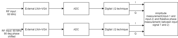
I am planning to use LNA as well variable gain amplifier with AGC mechanism at the input of RF-ADC , so that my dynamic input RF signal amplitude range will fall into the ADC full scale power. My input signal is pure sine wave RF signal.

But by doing so, using of external LNA and Variable gain amplifier with AGC , would it effect the phase of the input RF signal? can you please guide me ?
 

Hi, I don't really understand the question, since if you design RF receiver then you probably know that every block produce delay and phase shift. Even a single cable will produce additional phase shift, so yes, input RF signal's phase is affected by such a modification.
 

Hi,

Sorry for not elaborating the question properly. Actually , I want to make the compensation of all change in the input signal due to external components. and want to measure correct phase at the output ( in FPGA) . so, for that, I want to know, how would I measure the phase affection due to any external components like Amplifier
 

Well, you should share more technical details, it would be good to see that at least it is possible and necessary. I am not sure even your communication system is wireless for example, where the channel distortion can be massive and makes not too much sense to compensate such things.
Share please: system block figure, carrier freq, RF input bandwidth, modulation, ADC resolution and full scale, ADC sampling speed, required LNA+AGC gain and those part number, noise figure, IIP3, P1db, etc.
 

Hello,

No It is not a wireless system . I am talking about the Measurement system here. not some wireless communication system . So, the input interfacing is done through the RF cable only. which are phase stable. amnd also, the input signal is pure sine wave. no modulation. My aim is to receive pure sine wave signal, generate I,Q and measure accurate phase. ADC resolution is 14 bit. My input dynamic range is more than 40 dB.

LNA and VGA , I am searching , so it is TBD
--- Updated ---

Hello,

No It is not a wireless system . I am talking about the Measurement system here. not some wireless communication system . So, the input interfacing is done through the RF cable only. which are phase stable. amnd also, the input signal is pure sine wave. no modulation. My aim is to receive pure sine wave signal, generate I,Q and measure accurate phase. ADC resolution is 14 bit. My input dynamic range is more than 40 dB.

LNA and VGA , I am searching , so it is TBD
Frequency is up to 100 MHz. ADC full scale: -2.2 dBm, required max gain = 37 dB approx.
 
Last edited:

Nobody knows where the phase is. The only thing to do is to measure.
Because you cannot predict the AGC mechanism how it will respond. Because it's a feedback system and there will be many parameters to considered. (Poles, zeros, delay, settling, decay, phase shift, lagging, leading etc.)
Measurement is the best way.
 

Ok
Nobody knows where the phase is. The only thing to do is to measure.
Because you cannot predict the AGC mechanism how it will respond. Because it's a feedback system and there will be many parameters to considered. (Poles, zeros, delay, settling, decay, phase shift, lagging, leading etc.)
Measurement is the best way.
, So what you are trying to say is that, First I have to measure the phase change at the output of LNA and VGA , prepare a kind of look up table further to compensate the phase change done in external circuit.

As I have to measure the actual phase diff. between my 2 simultaneous same frequency input from I and Q samples.
so please let me know, if my above understanding is correct?
also, can you suggest a better way on the things that I can consider to select VGA and LNA that will induce minimum possible phase shifting effect on the signal.
 

As I have to measure the actual phase diff. between my 2 simultaneous same frequency input from I and Q samples.
I am still confused what are you looking for. Earlier you mentioned you have 1 pure sine wave which you would like to use to generate IQ signals with the knowledge of its absolute phase. Now you have 2, IQ input signals and you want to measure the phase difference between them?

Please share block figure of your measurement system, figures are so good, everybody love them.

Do you have specification for IQ phase error btw?
 

Ok

, So what you are trying to say is that, First I have to measure the phase change at the output of LNA and VGA , prepare a kind of look up table further to compensate the phase change done in external circuit.

As I have to measure the actual phase diff. between my 2 simultaneous same frequency input from I and Q samples.
so please let me know, if my above understanding is correct?
also, can you suggest a better way on the things that I can consider to select VGA and LNA that will induce minimum possible phase shifting effect on the signal.
You haven't remarked I/Q signals before. I thought that you got one signal to drive the ADC and you wanna attempt to compensate Input and Output.
Are you looking a simple solution to maintain the I/Q phases at the input of the ADC ? So that whatever the AGC level is, the I/Q signals will held 90 degree phase shift ? Right ?
 

Hello,

Sorry for all the misunderstanding and not elaborating the proper query. I have attached over here the basic block diagram of what I want to say.
As you can see, there are 2 simultaneous RF pure sine wave input signal , which have different amplitudes and they must be 90 deg apart.
Now , as external VGA(AGC), LNA are required to change the input signal's amplitude in such a way it falls into the ADC full scale power range. Now , As I know it is possible to read back the current External gain/loss to compensate all the changes I have made to the input signal that I can add in. But I am not quite sure about phase change and compensation in order to measure the correct phase diff. of the input signal.
This is one of the reference example. This difference between input signal's phase may be different , not 90 deg. and I want to measure that difference from the received I,Q samples.
I hope, now I have provided the detailed description of my question. Please provide guidance.
 

Attachments

  • basic diagram for understanding.png
    basic diagram for understanding.png
    19.3 KB · Views: 118

OK, now it's more obvious.
If you intend to maintain this 90 degree phase shift independent from amplifiers' gain settings, you can use
polyphase filter after the LNAs. Polyphase filter ( if the frequency is fixed and narrowband ) will guard the 90 degree phase shift between the signals whatever the gains ( I presumed the LNA gains are somehow different )
are. They are lossy circuits but if they are very well designed and implemented, they will keep this phase shift as 90 degree in any circumstance.
 

Hello,
Actually my input frequency will not be remain the same. For one single operation of time , it will be same. but then it will be variable. Also, 90 deg is given as an example. There may be any phase difference between 2 input signals within a range of 0-360 deg.
 

almost any sort of variable gain amplifier will change the phase of the signal as you vary the gain.
some more than others.

i suppose it could mess up beam forming in a phased array if it gets out of hand. so choose one that does not do it too much
 

    Maitry07

    Points: 2
    Helpful Answer Positive Rating
Status
Not open for further replies.

Part and Inventory Search

Welcome to EDABoard.com

Sponsor

Back
Top