T
treez
Guest

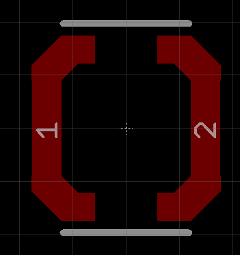
I have a SOT89 package on my 4 layer pcb. I made its unusual shaped footprint by sticking lots of polygons together.
When i gerber the board, eagle messages me, saying that this SOT89 package has unusual polygons, and that this is going to result in loads of plot data, and therefore do i really want to continue with the gerbering..........
i did notice that the top copper layer (where this package is) came out as 1MB in the gerbers, whereas other layers were less, eg the bottom layer was 603KB.
.......i am not sure why Eagle thought it necessary to message me like this.....what significance does it have?....does it mean more expense to get the board made up?

