Continue to Site

Welcome to EDAboard.com

Welcome to our site! EDAboard.com is an international Electronics Discussion Forum focused on EDA software, circuits, schematics, books, theory, papers, asic, pld, 8051, DSP, Network, RF, Analog Design, PCB, Service Manuals... and a whole lot more! To participate you need to register. Registration is free. Click here to register now.

dynamic shift register

Status
Not open for further replies.

andrea22

Junior Member level 2
Joined
Oct 1, 2010
Messages
21
Helped
1
Reputation
2
Reaction score
0
Trophy points
1,281
Activity points
1,427
Hi,
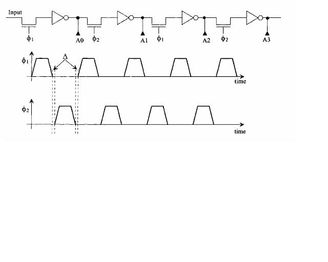
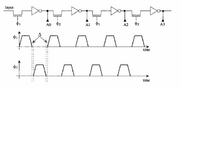
Does anyone know why are need non-overlapping clocks in dynamic shift register?
Or why this circuit doesn't work with overlapped clocks?
Can anyone draw timing diagrams in point A0,A1,A2,A3?
 

When the clocks overlap, all the pass transistors turns on at the same time, and the whole logic becomes a combinatorial buffer. No longer a shift register.
 

Do you have any literature about pass transistors?
Why when I simulated this circuit,when voltage on gate of pass
transistor is zero (0 V),I get that voltage at the output of pass transistor is
negative (small negative voltage)?
What I ment when Phi1=0 or Phi2=0?

When Phi1=Vdd and Vin=Vdd maximum voltage at the output of pass transistor is Vdd-Vtn?
How this effects on CMOS inverter?(inverters are realised in CMOS technology)
 
Last edited:

When Phi1=Vdd and Vin=Vdd maximum voltage at the output of pass transistor is Vdd-Vtn?
yes
How this effects on CMOS inverter?(inverters are realised in CMOS technology)
You have to design the inverter to make it work with the threshold accordingly.
 

These are my diagrams.The third diagrams is at the output of pass transistor.
What is happening when Phi1=0,Vin=Vdd and Phi1=0 and Vin=0?
 

Attachments

  • diagrams3.JPG
    diagrams3.JPG
    220.2 KB · Views: 76
Last edited:

Status
Not open for further replies.

Part and Inventory Search

Welcome to EDABoard.com

Sponsor

Back
Top