Continue to Site

Welcome to EDAboard.com

Welcome to our site! EDAboard.com is an international Electronics Discussion Forum focused on EDA software, circuits, schematics, books, theory, papers, asic, pld, 8051, DSP, Network, RF, Analog Design, PCB, Service Manuals... and a whole lot more! To participate you need to register. Registration is free. Click here to register now.

Dual Clock FIFO with controlled stream: Verilog

Status
Not open for further replies.

beginner_EDA

Full Member level 4
Joined
Aug 14, 2013
Messages
191
Helped
0
Reputation
0
Reaction score
0
Trophy points
1,296
Activity points
3,854
Hi,
I am using Dual Clock fifo from Altera IP Core and instantiating it as:


Code Verilog - [expand]
1
2
3
4
5
6
7
8
9
10
11
12
13
rx_dcfifo rx_dcfifo_inst (
        .aclr(),
    .data(payload),
    .rdclk(test_100_mhz),
    .rdreq(Rx_fifo_read),
    .wrclk(test_250_mhz),
    .wrreq(Rx_fifo_write),
    .q(Rx_output_from_fifo),
    .rdempty(Rx_fifo_empty),
    .rdusedw(r_depth_rx),
    .wrfull(Rx_fifo_full),
    .wrusedw(w_depth_rx)
    );


The input data width(data) is 4 bit at 250 MHz whereas output(q) data width is 8 bit at 100 MHz.

The continuous input stream is controlled by a trigger signal i.e. if trigger_signal == 1, then only write to fifo otherwise not.

I am struggling to understand how wrfull signal can be coordinate with trigger_signal while setting
wrreq <= 1 ?

Similarly how to coordinate rdempty signal with trigger_signal while setting rdreq <= 1 ?

I tried in this way:


Code Verilog - [expand]
1
2
3
4
5
6
7
8
9
10
11
12
13
14
15
16
17
18
19
20
21
22
23
24
25
26
always @ (posedge test_250_mhz) 
    begin
        if (trigger == 1)
            begin
                Rx_fifo_write <= 1;
                payload <= ENET0_RX_DATA;
            end
        if (trigger == 0) || (Rx_fifo_full ==  1)
                begin
                    Rx_fifo_write <= 0;
                end
    end
    
always @ (posedge test_100_mhz) 
begin
 
            if (trigger == 1)
               begin 
                  Rx_fifo_read <= 1;
                  //Rx_output_from_fifo
                end
            if (trigger == 0) || (Rx_fifo_empty == 1)
                begin
                    Rx_fifo_read <= 0;
                end
end


but I end up with some stale data on reading side and first 4 bits on writing side.

In VHDL, I think one can do this using FSM with 3 different processes, 1st process for clocked update of Present state, 2nd for State transition and 3rd for output decode.

but in verilog I am facing problem.

Any idea please?

Regards
 

you can do the same state machines in Verilog: https://www.altera.com/support/supp...mples/design-software/verilog/ver_statem.html

Why have you got a 4bit@250MHz/8bit@100MHz ratio? this means you going to be keeping the FIFO full a lot of the time and you are losing efficiency. The output rate (and input rate) is only 800Mbs (input could run at 1Gb/s)

What options have you specified when you created the FIFO. Did you turn underflow and overflow checking on? with these options you can just assert wrreq whenever data is available and use !wrfull to determin when to get the next dword. Same on the read side.
 

I tried in this way:

Code Verilog - [expand]
1
2
3
4
5
6
7
8
9
10
11
12
13
14
15
16
17
18
19
20
21
22
23
24
25
26
27
28
29
30
31
32
33
34
35
36
37
38
39
40
41
42
43
44
45
46
47
48
49
50
51
52
53
54
55
56
57
58
59
60
61
62
63
64
65
66
67
68
69
70
71
72
73
74
75
76
77
78
79
80
81
82
83
84
85
86
87
88
89
90
91
92
93
94
95
96
97
98
99
100
101
102
103
104
105
106
107
108
109
110
111
112
113
114
115
116
117
118
119
120
121
122
123
124
125
126
127
128
129
130
131
132
133
134
135
136
137
138
139
140
141
142
143
144
145
146
147
148
149
150
151
152
153
154
155
156
157
158
159
160
161
162
163
164
165
166
module test(
 
    //////////// CLOCK //////////
    CLOCK_50,
    CLOCK2_50,
    CLOCK3_50,
 
    //////////// LED //////////
    LEDG,
    LEDR,
 
    //////////// KEY //////////
    KEY,
 
    //////////// SW //////////
    SW,
 
    //////////// GPIO, GPIO connect to GPIO Default //////////
    GPIO 
);
 
//=======================================================
//  PARAMETER declarations
//=======================================================
 
 
//=======================================================
//  PORT declarations
//=======================================================
 
//////////// CLOCK //////////
input                       CLOCK_50;
input                       CLOCK2_50;
input                       CLOCK3_50;
 
//////////// LED //////////
output           [8:0]      LEDG;
output          [17:0]      LEDR;
 
//////////// KEY //////////
input            [3:0]      KEY;
 
//////////// SW //////////
input           [17:0]      SW;
 
//////////// GPIO, GPIO connect to GPIO Default //////////
inout   reg     [7:0]       GPIO;
 
 
reg [1:0] current_state,next_state ;
reg trigger;
 
parameter idle=0, write=1, read=2;
 
 
reg input_to_fifo;
reg areset_fifo;
wire reset;
wire fifo_rclk;
wire fifo_empty;
reg fifo_read;
reg fifo_write;
wire fifo_full;
wire  test_250_mhz, test_125_mhz, test_100_mhz, test_25_mhz, test_12p5_mhz;
wire [7:0]  output_from_fifo;
wire [11:0] r_depth;
wire [12:0] w_depth;
 
reg [3:0] ADC_DATA = 0; 
 
assign reset = (!KEY[0]);
 
always @(posedge test_250_mhz)
begin
ADC_DATA <= ADC_DATA + 1;
  if (ADC_DATA < 8)
  trigger <= 1;
  else
  trigger <= 0;
 
end
 
always @(posedge test_250_mhz or posedge reset)
begin
    if (reset == 1)
        current_state <= idle;
    else
        current_state <= next_state;    
end
 
 
always @(current_state) 
     begin
          case (current_state)
               idle:
                        begin
                   fifo_write <= 0;
                         fifo_read <= 0;
                        end
               write:
                   begin
                          fifo_write <= 1;
                         // input_to_fifo <= ADC_DATA;
                         end
                    read:
                            fifo_read <= 1;
               default:
                  ;  
                          
          endcase
     end
 
always @(current_state, trigger, fifo_empty, fifo_full)
     begin
             case (current_state)
                    idle:
                            begin 
                              if ((trigger) && (!fifo_full))
                                next_state= write;
                                else if ((trigger) || (!fifo_empty))
                                 next_state= read;  
                              end
                    write:                         
                                 if((fifo_full) || (!trigger))
                                 next_state= idle;
                          read:
                                 if ((fifo_empty) || (!trigger))
                         next_state= idle;
                          default:
                         next_state= idle;
               endcase
     end


pll_test pll_test (
    .inclk0(CLOCK_50),
    .c0(test_100_mhz),
    .c1(test_25_mhz),
    .c2(test_12p5_mhz),
    .c3(test_250_mhz),
    .c4(test_125_mhz)
    );


    dual_clock_fifo dual_clock_fifo_inst(
    .aclr(),
    .data(ADC_DATA),
    .rdclk(test_125_mhz),
    .rdreq(fifo_read),
    .wrclk(test_250_mhz),
    .wrreq(fifo_write),
    .q(output_from_fifo),
    .rdempty(fifo_empty),
    .rdusedw(r_depth),
    .wrfull(fifo_full),
    .wrusedw(w_depth)
    );    
      
    always @ (test_125_mhz) 
begin   
    GPIO <=   {output_from_fifo[3:0],output_from_fifo[7:4]} ;
end   
      
endmodule


but I couldn't manage transition state for reading. Any idea?
I took 250 MHz also for reading to observe it on signal tap. Do I need to write separate state machine for both writing to and reading from FIFO?

Why have you got a 4bit@250MHz/8bit@100MHz ratio?
Unfortunately, I have such combination. Is there any other way(apart from 125 MHz @ 8bit) to maintain 1Gb/s on receiving end.
Did you turn underflow and overflow checking on?
yes
 
Last edited:

Hi,

The input data width(data) is 4 bit at 250 MHz whereas output(q) data width is 8 bit at 100 MHz.
so input is 4 bit x 250MHz = 1GBit/s
and output is 8 bit x 100MHz = 0.8GBit/s.

The continuous input stream is controlled by a trigger signal i.e. if trigger_signal == 1, then only write to fifo otherwise not.
In my understanding the input data stream can´t be countinous.

And if you enable/disable data stream don´t you loose data?
(is this the meaning of your trigger signal? Then i don´t call it continous)

If you enable/disable it then most probably you need an "almost full" signal, because at this datarate you may need some headroom for data that is input to the FIFO after you disabled receiving data.

Klaus
 

Whatever you do here, unless the input has backpressure, you're going to lose data. There is nothing you can do about it if you data comes in any faster than 800Mb/s
 
Hi,
And if you enable/disable data stream don´t you loose data?
(is this the meaning of your trigger signal? Then i don´t call it continous)
Klaus

yes, you are right. wording is my mistake then. I am only interested with data as long as trigger signal is on.

I have trouble to formulate code to write at 250 MHz into dual clock fifo as long as trigger signal is high and read only this written data from fifo at 100 MHZ.
I tried as mentioned above using FSM but have no success.
Any help?
 

Hi,

i don´t understand your application.

It seems you have an ADC. (4 bit ADC is something unusual)
It should sample continously with a constant sample rate. (at least at most applications)
Then usually you write data to the FIFO with your ADC sample rate as long as the FIFO is not full.
If the FIFO is full you will loose data and therefore an error flag should be raised. --> your data is not valid.

You may read data with random speed, as long as there is data in the FIFO. The average read rate will be the same as the FIFO input rate (in bits/s).
--> here it makes no sense to use the same "trigger" signal for input and output of the FIFO. Input "trigger" is the ADC sample rate. Output "trigger" is a different signal depending on your applicatin.

Often this scenario is used when analog data is sampled and processed. Maybe for calculating an FFT.
Contiouns ADC sampling into FIFO, but bulk data transfer to FFT processor.

But we don´t know much about your application.

Klaus
 
Often this scenario is used when analog data is sampled and processed. Maybe for calculating an FFT.
Contiouns ADC sampling into FIFO, but bulk data transfer to FFT processor.

But we don´t know much about your application.

Klaus
Hi, Thanks for your valuable concept.
I have similar application as you mentioned. I would like to read ADC Sample, write only valid data into fifo and read it from FIFO at different clock rate for further processing. I have difficulty in reading FIFO. I end up with stale data. what I did on reading side:

Code Verilog - [expand]
1
2
3
4
5
6
7
always @(read_clk)
begin
if (!fifo_empty)
fifo_read <= 1;
else
fifo_read <= 0;
end


but I still got stale data at output (q pin) of FIFO.
What could be the reason?
 

Hi,

What reads your FIFO data?

If it is a controller, then FIFO_read should be the same (or driven from) your controller_read line.

Again: We don´t know much about your application.
Maybe it´s time to give a description.

Klaus
 

Hi,
To check first whether It is right or not, I am observing it in signal Tap, but later intended for another component of processing.
 

It is odd that you use trigger in both clock domains -- 250Mhz is 4ns, 100Mhz is 10ns, the worst case edge-to-edge is 2ns.

You also use the empty signal in a clocked process to generate a read. On the last read, the fifo read signal is asserted, and empty is not asserted. The next-state logic for the fifo read _register_ says to keep reading. On the next cycle, the fifo read will be asserted and the fifo will be empty.

The same for the write logic, it will be delayed by one cycle at the beginning and will attempt to write an additional word.

dual-clock fifos can have annoying behavior in terms of flag generation. There can be a few cycles of latency between when the fifo is written and the flags show the fifo as not empty.

If you need 1Gbps, you would need to use 10+ bits for the output of the fifo. probably 16 bit @ 100MHz.

You have a state machine that uses signals from 100MHz and 250MHz. These cross-domain paths are at best 2ns paths.

It looks like you just want to write until the fifo is full, then read until it is empty. This limits the data rate to something less than 500Mbps.
 

Also, your trigger lasts for 4ns. It is possible for it to be entirely missed by the 100MHz clock which has a 10ns period.
 

Hi,

I just wonder if it makes sense to use different input and output bus width.

I'd use an input stage that forms 4 x 4 bits to one 16 bit word, then -if complete - it is transferred to the 16 bit wide FIFO.
To ensure full data rate you may need it to be double buffered. (2 x 16 bits registers).
The FIFO access is more relaxed then: 1Gbit/s = 66MWords x 16 bits.

Klaus
 

Multiple posts have been giving the OP a false sense of the 100 MHz 250 MHz clock domain transfer timing.

It's never been stated that the 100 MHz and 250 MHz domains are frequency locked, therefore any timing relationship can not be determined and the comments about 2 ns being the worst case is meaningless. The clocks will drift in phase with respect to each other if they are source from different clock oscillators.

What should be said is any control signals that cross the clock domains needs to be properly synchronized (a minimum of 2 FFs strung together).

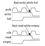
Synchronous descriptions for the read gating of the empty and the write gating of the full result in the problem shown in the figure below.
Capture.JPG
In both cases the result is an extra read and write are allowed. To avoid this the full/empty flags can be gated directly with the write/read from the control logic.

Code:
rx_dcfifo rx_dcfifo_inst (
    .aclr(),
    .data(payload),
    .rdclk(test_100_mhz),
    [COLOR="#FF0000"].rdreq(Rx_fifo_read && !Rx_fifo_empty)[/COLOR],
    .wrclk(test_250_mhz),
    [COLOR="#FF0000"].wrreq(Rx_fifo_write && !Rx_fifo_full),[/COLOR]
    .q(Rx_output_from_fifo),
    .rdempty(Rx_fifo_empty),
    .rdusedw(r_depth_rx),
    .wrfull(Rx_fifo_full),
    .wrusedw(w_depth_rx)
    );
However you should note that this may become a critical path in the timing depending on whether the empty/full logic is generated by combinational logic (i.e. address pointer comparison).
 
Post #3 shows them coming from the same PLL.

Almost certainly better to treat them as independent either way.
 

Post #3 shows them coming from the same PLL.
Ah, I see that now, didn't actually look at their code very carefully.

Almost certainly better to treat them as independent either way.
I'm in complete agreement, the beat between the two different clock domains puts a very difficult setup timing constraint on any transfers between the domains, not worth the effort of dealing with timing closure problems, better to synchronize and add false path constraints and/or maximum path delay constraints for those CDC FFs.
 

the beat between the two different clock domains puts a very difficult setup timing constraint on any transfers between the domains, not worth the effort of dealing with timing closure problems, better to synchronize and add false path constraints and/or maximum path delay constraints for those CDC FFs.
Hi,
your suggestion to use for write and read request:
.wrreq(Rx_fifo_write && !Rx_fifo_full) and
.rdreq(Rx_fifo_read && !Rx_fifo_empty)
have solved my problem.
But some time (one in 10 times you can say), I have this issue:
Input 4 bit:
4h
5h
6h
7h
...
then output 8 bit is:
4xh
65h
x7h
where x is previous/later/unknown value.

[Most of the time output is:
54h
76h
]

Does this little uncertainty is due to SDC timing constraints what you described here?

or do I need to you clock crossing but I guess it is not senseful for fifo here.

or is there anything else?

regards
 

Then start debugging the problem, we don't have your testbench or the current design, so anything said is purely conjecture.

To debug the design at minimum you need to do the following.

1. put all the signals of the FIFO interface in the waveform view of your simulator, along with the logic that makes up your FIFO control.
2. Run the simulation
3. observe when the data is read and when it is written and the flags (is it correct).

The problem you are describing seems to indicate the FIFO is being written with bad data, which means your write control logic is probably to blame. I've never seen a problem when using Xilinx's (or Altera) width changing FIFOs where the read side reports it's not empty when only part of the read data is written.

If you at least run a simulation with the waveforms you can post the waveform image here and we can take a look.
 

If you at least run a simulation with the waveforms you can post the waveform image here and we can take a look.
In attachment there is a waveform observed in signal tap clocked at 250 MHz: 4 bit(equal to write freq) for the ASCII input abcdefghijkl and showing corresponding hex values there.

P.S. the read clock is 100 MHz @ 8 bit.

- - - Updated - - -

Similary, in attchment waveform (fifo_error_read.jpg) of signal tap clocked at 100 MHz:8 bit(equal to read freq and the write clock here is 250 MHz @ 4 bit. ) is also shown here for comparison.
 

Attachments

  • fifo_error_2.jpg
    fifo_error_2.jpg
    488.3 KB · Views: 72
  • fifo_error_read.jpg
    fifo_error_read.jpg
    460.1 KB · Views: 76
Last edited:

Why didn't you run a simulation on the design before implementing it? Debugging a design with signal tap is what you do when the simulation doesn't show any problem, but the errors only occur when the design is implemented. It's not a crutch for doing what should have been up front design and simulation...BEFORE implementation.

This is the reason so many FPGA designs I've been called in to fix are basically throw away designs that should be started from scratch.

Because you used signal tap to debug you have absolutely no idea what is the relationship between writing with a 250 MHz clock and reading with a 100 MHz clock as you can either capture in one or the other clock domain, but don't know anything about the relative timing of the two. Which means you've probably got an extra read/write occurring as the FIFO toggles between empty/not_empty.

And explain to me where the error in the sequence is...I don't see it in fifo_error_read.jpg.

Capture.JPG

This starts with a (0x61) and ends on l (0x6c), and doesn't skip or repeat.

So once again what is wrong with the reads?

Looking at fifo_error_2.jpg...Maybe you don't understand if you over sample a 100 MHz bus at 250 MHz you'll end up with repeated values showing up. Once again using signal tap to simulate/debug a design is downright ridiculous and if you do use it you better know what you are doing and why you are doing it.
 
Status
Not open for further replies.

Part and Inventory Search

Welcome to EDABoard.com

Sponsor

Back
Top