Continue to Site

Welcome to EDAboard.com

Welcome to our site! EDAboard.com is an international Electronics Discussion Forum focused on EDA software, circuits, schematics, books, theory, papers, asic, pld, 8051, DSP, Network, RF, Analog Design, PCB, Service Manuals... and a whole lot more! To participate you need to register. Registration is free. Click here to register now.

[PIC] dsPIC33EP512MU810 UART Module not working

Status
Not open for further replies.

nairitb

Junior Member level 1
Joined
Mar 25, 2014
Messages
18
Helped
0
Reputation
0
Reaction score
0
Trophy points
1
Activity points
154
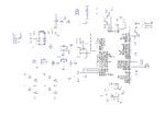
I am using a prototype board designed and fabricated by me. Crystal is 24MHz.

Board is working. Can blink LEDs and enable PWM module.

However, I am currently stuck in UART module. I am connecting "U1Tx To Pin RP64" & "U1Rx To Pin RPI75". The program is to receive data from pc and if the received byte is "a" then transmit "b" back to pc. Its not working.

The debugger (ICD3) is not working for this program (dont know why). So I decided to use LEDs connected at RF0, RF1, RF2 & RF3 to see where the program gets stuck. Found that the program gets stuck at if(U1STAbits.FERR == 1) indicating "Framing error has been detected for the current character". But I did not send any data from the pc.

LEDs connected at RF0 & RF2 are ON but LEDs connected at RF1 & RF3 are OFF.

Can someone please look into the program and point out my mistake?

Code:
// Crytal is 24MHz.
// Configure the oscillator to operate the device at 51 MIPS using PLL

#define _XTAL_FREQ 24000000
#define FOSC (102000000)
#define FCY (FOSC/2)

//#if defined(__dsPIC33E__)
//#include "p33exxxx.h"
//#endif
#include <stdio.h>
#include <stdlib.h>
#include <p33EP512MU810.h>
//#include <delay.h>
#include <libpic30.h>

// DSPIC33EP512MU810 Configuration Bit Settings


// FGS
#pragma config GWRP = OFF // General Segment Write-Protect bit (General Segment may be written)
#pragma config GSS = OFF // General Segment Code-Protect bit (General Segment Code protect is disabled)
#pragma config GSSK = OFF // General Segment Key bits (General Segment Write Protection and Code Protection is Disabled)


// FOSCSEL
#pragma config FNOSC = PRIPLL // Initial Oscillator Source Selection Bits (Internal Fast RC (FRC))
#pragma config IESO = ON // Two-speed Oscillator Start-up Enable bit (Start up with user-selected oscillator source)


// FOSC
#pragma config POSCMD = HS // Primary Oscillator Mode Select bits (HS Crystal Oscillator Mode)
#pragma config OSCIOFNC = OFF // OSC2 Pin Function bit (OSC2 is clock output)
#pragma config IOL1WAY = OFF // Peripheral pin select configuration (Allow only one reconfiguration)
#pragma config FCKSM = CSECMD // Clock Switching Mode bits (Both Clock switching and Fail-safe Clock Monitor are disabled)


// FWDT
#pragma config WDTPOST = PS32768 // Watchdog Timer Postscaler Bits (1:32,768)
#pragma config WDTPRE = PR128 // Watchdog Timer Prescaler bit (1:128)
#pragma config PLLKEN = OFF // PLL Lock Wait Enable bit (Clock switch to PLL source will wait until the PLL lock signal is valid.)
#pragma config WINDIS = OFF // Watchdog Timer Window Enable bit (Watchdog Timer in Non-Window mode)
#pragma config FWDTEN = OFF // Watchdog Timer Enable bit (Watchdog timer enabled/disabled by user software)


// FPOR
#pragma config FPWRT = PWR128 // Power-on Reset Timer Value Select bits (128ms)
#pragma config BOREN = OFF // Brown-out Reset (BOR) Detection Enable bit (BOR is disabled)
#pragma config ALTI2C1 = OFF // Alternate I2C pins for I2C1 (SDA1/SCK1 pins are selected as the I/O pins for I2C1)
#pragma config ALTI2C2 = OFF // Alternate I2C pins for I2C2 (SDA2/SCK2 pins are selected as the I/O pins for I2C2)


// FICD
#pragma config ICS = PGD3 // ICD Communication Channel Select bits (Communicate on PGEC3 and PGED3)
#pragma config RSTPRI = PF // Reset Target Vector Select bit (Device will obtain reset instruction from Primary flash)
#pragma config JTAGEN = OFF // JTAG Enable bit (JTAG is disabled)


// FAS
#pragma config AWRP = OFF // Auxiliary Segment Write-protect bit (Auxiliary program memory is not write-protected)
#pragma config APL = OFF // Auxiliary Segment Code-protect bit (Aux Flash Code protect is disabled)
#pragma config APLK = OFF // Auxiliary Segment Key bits (Aux Flash Write Protection and Code Protection is Disabled)

#define FP 51000000
#define BAUDRATE 9600
#define BRGVAL ((FP/BAUDRATE)/16) - 1

int main(void)
{


// Disable Watch Dog Timer

RCONbits.SWDTEN=0;

TRISF=0;


// Configure PLL prescaler, PLL postscaler, PLL divisor
PLLFBD= 32; // M=34
CLKDIVbits.PLLPOST= 0; // N2=2
CLKDIVbits.PLLPRE= 2; // N1=4


// Initiate Clock Switch to Primary Oscillator with PLL (NOSC=0b011)

//Oscillator select
__builtin_write_OSCCONH(0x03);

// Clock Switch
__builtin_write_OSCCONL(OSCCON | 0x01); //turn on OSWEN

while (OSCCONbits.OSWEN); //wait until OSWEN to low

// Wait for Clock switch to occur
while (OSCCONbits.COSC!= 0b011);

// Wait for PLL to lock
while (OSCCONbits.LOCK!= 1);

PORTFbits.RF2 = 1;

// Configure Input Functions
//*************************************************************

//OSCCONL Unlock Sequence
__builtin_write_OSCCONL(0x46);
__builtin_write_OSCCONL(0x57);

// Assign U1Rx To Pin RPI75
//***************************
RPINR18bits.U1RXR = 0x4B;
//***************************
//*************************************************************

// Configure Output Functions
//*************************************************************

// Assign U1Tx To Pin RP64
//***************************
RPOR0bits.RP64R = 1;
//***************************

//Set IOLOCK as a single operation.
OSCCONbits.IOLOCK = 1;

PORTFbits.RF0 = 1;
// Configure oscillator as needed
U1MODEbits.STSEL = 0; // 1-stop bit
U1MODEbits.PDSEL = 0; // No Parity, 8-data bits
U1MODEbits.ABAUD = 0; // Auto-Baud disabled
U1MODEbits.BRGH = 0; // Standard-Speed mode
U1BRG = BRGVAL; // Baud Rate setting for 9600
U1STAbits.URXISEL = 0; // Interrupt after one RX character is received;
U1MODEbits.UARTEN = 1; // Enable UART

char ReceivedChar;

while(1)
{
while(U1STAbits.URXDA == 0);

/* Check for receive errors */
if(U1STAbits.FERR == 1)
{
continue;
PORTFbits.RF3 = 1;
}

/* Must clear the overrun error to keep UART receiving */
if(U1STAbits.OERR == 1)
{
U1STAbits.OERR = 0;
continue;
}

/* Get the data */
//if(U1STAbits.URXDA == 1)
//{
ReceivedChar = U1RXREG;
//}

if(ReceivedChar == 'a')
{
PORTFbits.RF1 = 1;

U1STAbits.UTXISEL0 = 0; // Interrupt after one TX character is transmitted
U1STAbits.UTXISEL1 = 0;
IEC0bits.U1TXIE = 1; // Enable UART TX interrupt
U1MODEbits.UARTEN = 1; // Enable UART
U1STAbits.UTXEN = 1; // Enable UART TX

U1TXREG = 'b';
}
}
}

Thanks and regards,
Nairit
 

dsPIC33EP512MU810 UART Module not working .
First advice dspic o/p is ttl 0:3.5 volts . PC serial port is -/+ 9 volts > use max 232 Ic to adjust leveling.
second one: do calculate the PLL for that dspic ic
send an image or schmatic for more details
hope it helps
Zeyad
 
check your calculation for the required FOSC (102000000)

using your values of PLLpre, PLLpost, etc I get FOSC (108000000)

to get FOSC (102000000) I think PLdiv should be 32

to test the UART I would have a loop transmitting a character to PC
you can at least see if something is being received even if it is rubbish
if you have an oscilloscope you can check the bit rate etc is corrrect
 
Last edited:

I am using MAX232 for Serial comm with pc. Board schematic attached.

PLL calculations are as follows:

1. To execute instructions at 51 MHz, ensure that the required system clock frequency is:
FOSC = 2 x FCY = 102 MHz

2. To set up the PLL and meet the requirements of the PLL, follow these steps:

a) Select the PLL postscaler to meet the VCO output frequency requirement (120 MHz < FSYS < 340 MHz).
• Select a PLL postscaler ratio of N2 = 2
• Ensure that FSYS = (FOSC x N2) = 204 MHz

b) Select the PLL prescaler to meet the PFD input frequency requirement (0.8 MHz < FPLLI < 8.0 MHz).
• Select a PLL prescaler ratio of N1 = 4
• Ensure that FPLLI = (FIN ÷ N1) = (24 ÷ 4) = 6 MHz

c) Select the PLL feedback divisor to generate the required VCO output frequency based on the PFD input frequency.
• FSYS = FPLLI x M
• M = FSYS ÷ FPLLI = 204 ÷ 6 = 34

So,
PLLFBD= 32; // M=34
CLKDIVbits.PLLPOST= 0; // N2=2
CLKDIVbits.PLLPRE= 2; // N1=4

Am I missing something?
 

Attachments

  • Controller Schematic.jpg
    Controller Schematic.jpg
    758.2 KB · Views: 158

Ignore my last post - I had misread your code !

did you try transmitting characters to the PC to see if anything was being received?
 

Yes horace.

I tried transmitting. I am using HyperTerminal in pc to check if anything is being received. Nothing

I think I have not configured HyperTerminal correctly or else my peripheral pin selection code is not working.

For PPS, earlier I wrote:

Code:
// Configure Input Functions
//*************************************************************

//OSCCONL Unlock Sequence
__builtin_write_OSCCONL(0x46);
__builtin_write_OSCCONL(0x57);

// Assign U1Rx To Pin RPI75
//***************************
RPINR18bits.U1RXR = 0x4B;
//***************************
//*************************************************************

// Configure Output Functions
//*************************************************************

// Assign U1Tx To Pin RP64
//***************************
RPOR0bits.RP64R = 1;
//***************************

//Set IOLOCK as a single operation.
OSCCONbits.IOLOCK = 1;

Now I have changed it to:

Code:
// unlock the registers, then use PPS to config port pins to be used by SPI
    PPSUnLock;    // this is a macro, do NOT use () at the end!
    iPPSInput(IN_FN_PPS_U1RX,IN_PIN_PPS_RPI75);
    iPPSOutput(OUT_FN_PPS_U1TX,OUT_PIN_PPS_RP64);
    PPSLock;    // this is a macro, do NOT use () at the end!

Here, IN_PIN_PPS_RPI75 is returning error when compiling. I tried IN_PIN_PPS_RP75. Compiled without errors. So I think it has to do with RPI thing. Dont know how to correct it :thinker: Am I missing something?

Thanks
 

a) If URXINV = 0, use a pull-up resistor on the
RX pin.
b) If URXINV = 1, use a pull-down resistor on
the RX pin.
 

I found out a peculiar thing:

When I use iPPSInput(IN_FN_PPS_U1RX,IN_PIN_PPS_RPI34); or a lower RPI (33, 32 ...) its compiling.

But when I go to a higher pin number (>34), say iPPSInput(IN_FN_PPS_U1RX,IN_PIN_PPS_RPI35); or iPPSInput(IN_FN_PPS_U1RX,IN_PIN_PPS_RPI75); its not compiling.

Any explanation for this behaviour?

@milan.rajik: I did not understand your post. Can you please elaborate a little?

- - - Updated - - -

PPS.H header file in my xc16 installation folder attached herewith. View attachment pps.txt

Changed file type to .txt as .h was not getting uploaded. Either way, it opens in notepad. So no problem.

peripheralversion.h also attached. View attachment peripheralversion.txt
 
Last edited:

in the dsPIC33EP512MU810 data sheet
https://ww1.microchip.com/downloads/en/DeviceDoc/70616g.pdf

the dsPIC33EP512MU810 100 pin TQFP diagram show RPI35 on pin 22

however the version of pps.h I have does not define RPI35 - it has
Code:
#define IN_PIN_PPS_RPI34			34					/* Assign RPI34 as Input Pin */
#define IN_PIN_PPS_RP35				35					/* Assign RP35 as Input Pin */
which defines RP35

perhaps post an question of the Microchip forum?
 

If UART Invert is selected then pull down resistor on Rx line. If not then use pull up.
 

The following code is working for me. Only transmitting, no receiving. Transmitting 'N'

Code:
// Crytal is 24MHz.
// Configure the oscillator to operate the device at 51 MIPS using PLL

#define _XTAL_FREQ  24000000
#define FOSC    (102000000)
#define FCY     (FOSC/2)
#define  PPSUnLock
#define  PPSLock

//#if defined(__dsPIC33E__)
//#include "p33exxxx.h"
//#endif
#include <stdio.h>
#include <stdlib.h>
#include <p33EP512MU810.h>
#include <libpic30.h>
#include <pps.h>

// DSPIC33EP512MU810 Configuration Bit Settings


// FGS
#pragma config GWRP = OFF               // General Segment Write-Protect bit (General Segment may be written)
#pragma config GSS = OFF                // General Segment Code-Protect bit (General Segment Code protect is disabled)
#pragma config GSSK = OFF               // General Segment Key bits (General Segment Write Protection and Code Protection is Disabled)


// FOSCSEL
#pragma config FNOSC = PRIPLL           // Initial Oscillator Source Selection Bits (Internal Fast RC (FRC))
#pragma config IESO = ON               // Two-speed Oscillator Start-up Enable bit (Start up with user-selected oscillator source)


// FOSC
#pragma config POSCMD = HS              // Primary Oscillator Mode Select bits (HS Crystal Oscillator Mode)
#pragma config OSCIOFNC = OFF           // OSC2 Pin Function bit (OSC2 is clock output)
#pragma config IOL1WAY = OFF             // Peripheral pin select configuration (Allow only one reconfiguration)
#pragma config FCKSM = CSECMD           // Clock Switching Mode bits (Both Clock switching and Fail-safe Clock Monitor are disabled)


// FWDT
#pragma config WDTPOST = PS32768        // Watchdog Timer Postscaler Bits (1:32,768)
#pragma config WDTPRE = PR128           // Watchdog Timer Prescaler bit (1:128)
#pragma config PLLKEN = OFF              // PLL Lock Wait Enable bit (Clock switch to PLL source will wait until the PLL lock signal is valid.)
#pragma config WINDIS = OFF             // Watchdog Timer Window Enable bit (Watchdog Timer in Non-Window mode)
#pragma config FWDTEN = OFF             // Watchdog Timer Enable bit (Watchdog timer enabled/disabled by user software)


// FPOR
#pragma config FPWRT = PWR128           // Power-on Reset Timer Value Select bits (128ms)
#pragma config BOREN = OFF              // Brown-out Reset (BOR) Detection Enable bit (BOR is disabled)
#pragma config ALTI2C1 = OFF            // Alternate I2C pins for I2C1 (SDA1/SCK1 pins are selected as the I/O pins for I2C1)
#pragma config ALTI2C2 = OFF            // Alternate I2C pins for I2C2 (SDA2/SCK2 pins are selected as the I/O pins for I2C2)


// FICD
#pragma config ICS = PGD3               // ICD Communication Channel Select bits (Communicate on PGEC3 and PGED3)
#pragma config RSTPRI = PF              // Reset Target Vector Select bit (Device will obtain reset instruction from Primary flash)
#pragma config JTAGEN = OFF             // JTAG Enable bit (JTAG is disabled)


// FAS
#pragma config AWRP = OFF               // Auxiliary Segment Write-protect bit (Auxiliary program memory is not write-protected)
#pragma config APL = OFF                // Auxiliary Segment Code-protect bit (Aux Flash Code protect is disabled)
#pragma config APLK = OFF               // Auxiliary Segment Key bits (Aux Flash Write Protection and Code Protection is Disabled)

#define FP 51000000
#define BAUDRATE 9600
#define BRGVAL ((FP/BAUDRATE)/16) - 1

void main(void)
{

// Disable Watch Dog Timer

RCONbits.SWDTEN=0;

TRISF=0;


// Configure PLL prescaler, PLL postscaler, PLL divisor
PLLFBD= 32; // M=34
CLKDIVbits.PLLPOST= 0; // N2=2
CLKDIVbits.PLLPRE= 2; // N1=4

// Initiate Clock Switch to Primary Oscillator with PLL (NOSC=0b011)

//Oscillator select
__builtin_write_OSCCONH(0x03);

// Clock Switch
__builtin_write_OSCCONL(OSCCON | 0x01);  //turn on OSWEN

while (OSCCONbits.OSWEN); //wait until OSWEN to low

// Wait for Clock switch to occur
while (OSCCONbits.COSC!= 0b011);

// Wait for PLL to lock
while (OSCCONbits.LOCK!= 1);

// This is an EXAMPLE, so brutal typing goes into explaining all bit sets

	// The HPC16 board has a DB9 connector wired to UART2, so we will
	// be configuring this port only

	// configure U2MODE
	U2MODEbits.UARTEN = 0;	// Bit15 TX, RX DISABLED, ENABLE at end of func
	//U2MODEbits.notimplemented;	// Bit14
	U2MODEbits.USIDL = 0;	// Bit13 Continue in Idle
	U2MODEbits.IREN = 0;	// Bit12 No IR translation
	U2MODEbits.RTSMD = 1;	// Bit11 Simplex Mode
	//U2MODEbits.notimplemented;	// Bit10
	U2MODEbits.UEN = 0;		// Bits8,9 TX,RX enabled, CTS,RTS not
	U2MODEbits.WAKE = 0;	// Bit7 No Wake up (since we don't sleep here)
	U2MODEbits.LPBACK = 0;	// Bit6 No Loop Back
	U2MODEbits.ABAUD = 0;	// Bit5 No Autobaud (would require sending '55')

	U2MODEbits.BRGH = 0;	// Bit3 16 clocks per bit period
	U2MODEbits.PDSEL = 0;	// Bits1,2 8bit, No Parity
	U2MODEbits.STSEL = 0;	// Bit0 One Stop Bit

	// Load a value into Baud Rate Generator.  Example is for 9600.
	// See section 19.3.1 of datasheet.
	//  U2BRG = (Fcy/(16*BaudRate))-1
	//  U2BRG = (37M/(16*9600))-1
	//  U2BRG = 240
	U2BRG = BRGVAL;	// 40Mhz osc, 9600 Baud

	// Load all values in for U1STA SFR
	U2STAbits.UTXISEL1 = 0;	//Bit15 Int when Char is transferred (1/2 config!)
	U2STAbits.UTXINV = 0;	//Bit14 N/A, IRDA config
	U2STAbits.UTXISEL0 = 0;	//Bit13 Other half of Bit15
	//U2STAbits.notimplemented = 0;	//Bit12
	U2STAbits.UTXBRK = 0;	//Bit11 Disabled
	U2STAbits.UTXEN = 0;	//Bit10 TX pins controlled by periph
	U2STAbits.UTXBF = 0;	//Bit9 *Read Only Bit*
	U2STAbits.TRMT = 0;	//Bit8 *Read Only bit*
	U2STAbits.URXISEL = 0;	//Bits6,7 Int. on character recieved
	U2STAbits.ADDEN = 0;	//Bit5 Address Detect Disabled
	//U2STAbits.RIDLE = 0;	//Bit4 *Read Only Bit*
	//U2STAbits.PERR = 0;		//Bit3 *Read Only Bit*
	//U2STAbits.FERR = 0;		//Bit2 *Read Only Bit*
	U2STAbits.OERR = 0;		//Bit1 *Read Only Bit*
	//U2STAbits.URXDA = 0;	//Bit0 *Read Only Bit*

	//IPC7 = 0x4400;	// Mid Range Interrupt Priority level, no urgent reason

	//IFS1bits.U2TXIF = 0;	// Clear the Transmit Interrupt Flag
	//IEC1bits.U2TXIE = 1;	// Enable Transmit Interrupts
	//IFS1bits.U2RXIF = 0;	// Clear the Recieve Interrupt Flag
	//IEC1bits.U2RXIE = 1;	// Enable Recieve Interrupts


	RPOR0bits.RP64R = 3;		//RP64 as U2TX

	U2MODEbits.UARTEN = 1;	// And turn the peripheral on

	U2STAbits.UTXEN = 1;
while(1)
{
U2TXREG = 'N';
PORTFbits.RF3 = 1;
__delay_ms(500);
PORTFbits.RF3 = 0;
__delay_ms(500);
}
}

Checking in HyperTerminal. 'N' is received in COM1.

However, ICD3 not debugging. Its says:
Launching
Programming target
User program running
No source code lines were found at current PC 0x0
User program stopped


Now will try to receive data and send back to pc.

Thanks
 

Status
Not open for further replies.

Part and Inventory Search

Welcome to EDABoard.com

Sponsor

Back
Top