Continue to Site

Welcome to EDAboard.com

Welcome to our site! EDAboard.com is an international Electronics Discussion Forum focused on EDA software, circuits, schematics, books, theory, papers, asic, pld, 8051, DSP, Network, RF, Analog Design, PCB, Service Manuals... and a whole lot more! To participate you need to register. Registration is free. Click here to register now.

drill size PCB - EAGLE Cad

Status
Not open for further replies.

denver56

Member level 3
Joined
Mar 18, 2012
Messages
67
Helped
0
Reputation
0
Reaction score
0
Trophy points
1,286
Activity points
1,725
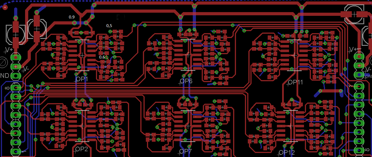
Hello people. I am currently developping a PCB for signal eleaboration with EAGLE software. I used 0.8128mm , 0.4064mm and 0.254mm width wires. I respectively used 0.9 , 0.6 and 0.5 round drills. What do you think about it ?
2) Unfortonately I exchange somo 0.6 with 0.5 drills so there are some 0.4064 wires with 0,5 drills and 0,254 wires with 0,6 drills. Is it a problem or I have to change these drills?
Thank you very much
 

Assuming you have a sensible pad/via size, the drill being larger than the track doesn't matter. For example, if you have a 0.3mm drill with a 0.15mm track it is fine as long as you have a 0.6mm pad, depending on the capability of your PCB supplier. Upload your PCB file or at least an image of the pads you think are a problem if you are still in doubt.

Keith
 
here you are ! of course if you notice others problems regarding pcb pls tell me them !! Thank you very much !
Next week I am going to send it to produce by a manufacturer !
 

You really need to run a DRC. Ignoring the unconnected nets (which technically are connected by overlapping but Eagle doesn't think so) I suspect you have some serious design rule violations. In particular, clearances which are far too small. Some of your oversized holes may give annulus violations.

Keith
 
DRC doesn't show any errors. Where you think should I notice clearance error? Can you post somo marks on the image ? THX!
 

Maybe it is just the scale of the image, but it depends on what design rules you have set. You definitely have lots of unconnected nets. If you post your board file I can check.

Keith
 
well, due to university policy I cannot attach the .brd. However I can post a High resolution image. Can you take a look and tell me if there are any problems/errors/advices for the PCB?
THANK YOU VERY MUCH!
 

Attachments

  • PCB.zip
    1.3 MB · Views: 119

Yes, I would be happy to take a look. It would be useful if you show a dimension so I can judge gaps from it (or post at a specific number of pixels per mm).

Keith.
 
ok just a second that i re-edit the image!

- - - Updated - - -

here you are !

- - - Updated - - -

here you are !
 

Attachments

  • pcb2.zip
    1,001.2 KB · Views: 117

That looks OK provided you are having the PCB made by someone who can handle 0.15mm minimum gap (that is what I am measuring from the image). The annulus that I was concerned about is at least 0.2mm which should be within the capabilities of most companies.

Check that your ground plane works ok when you fill it. There is the odd floating track on the bottom such as near OP10. If it isn't connected to the same net as the ground plane then it will create an island .

Ideally you would connect all the unconnected ratsnests (the small yellow lines on a lot of the pads) otherwise if you rely on the ground plane to make a connection and there is an island it may not be connected but you wouldn't notice due to the dozens of unconnected nets anyway. Normally I would expect my board to show as no unconnected nets when I have finished.

Keith
 
Any board will pass a DRC if you set the gaps to be extremely small.

IMO this board has too fine a gap between pads etc, this gap needs increasing considerably.
And there is plenty of room to do so.

These small gaps are completely unnecessary and are going to increase the cost of the board unnecessarily.
Have the components not got a component courtyard around them?

Also the vias on the thick tracks - the pads are too small for those size holes.
IMO - rip it up and start again, move the component further apart.
And for neatness make those columns of resistors etc all aligned - it wont look such a mess then.

EDIT: The hi res picture looks to have a little larger gaps however they are IMO still too close given the available space.
And for hecks sake - run a DRC that also includes acid traps, unfinished connections.
 
tanks for helping me ! I didn't understand what cyberrat mean when says :"Also the vias on the thick tracks - the pads are too small for those size holes.". Which pads do you mean? And what are "acid traps"?
moreover, which version of linking do you think is better in order to avoide noise/other problems ?
And which is the correct ratio of drills size / wire width ?
THX!
Thanks! ver1.PNGver2.PNG
 
Last edited:

The thick power supply tracks - its my opinion that for the hole size - the size of the pad is too small.
They may be OK - it just looks too small for a good annular ring. (google it).
I think that the via hole can actually be a lot smaller - what current is the circuit taking?

Re acid traps - try this link

Is this a one off pcb or are you planning on making many?
 
just two of them, why ?
moreover, which of the two versions do you think is better? THX!ver2.PNGver1.PNG
 

Status
Not open for further replies.

Part and Inventory Search

Welcome to EDABoard.com

Sponsor

Back
Top