elecs_gene
Member level 2
Hi,
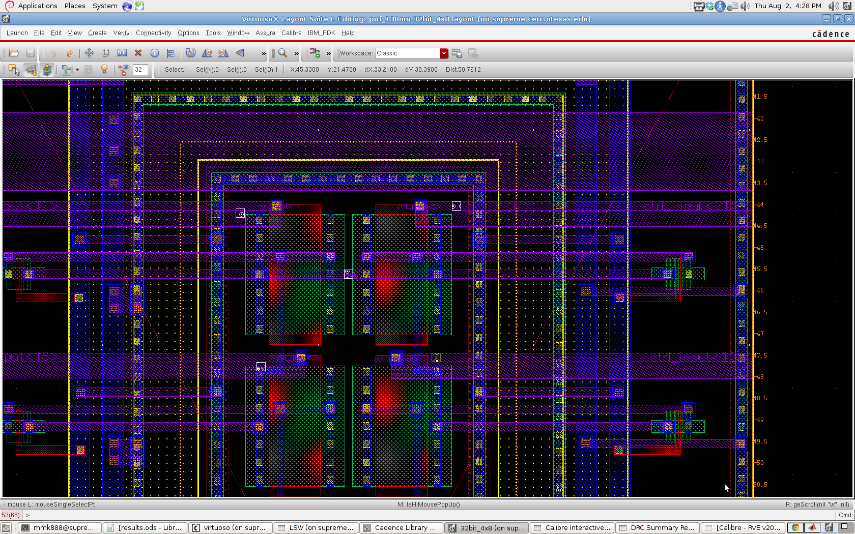
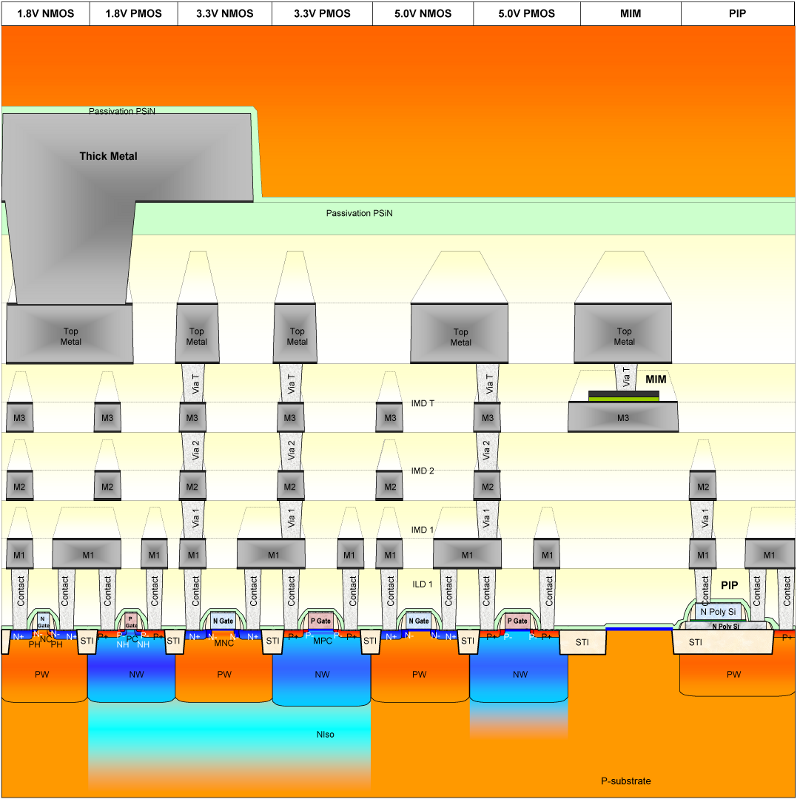
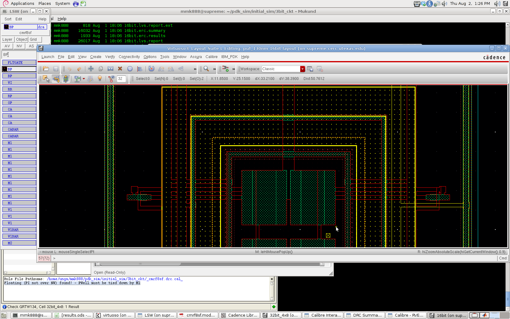
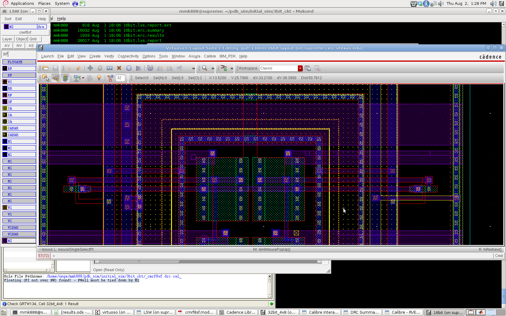
I am designing a circuit that uses an isolated P-well in IBM 130 nm. To create the isolated Pwell, I used a PI layer and a N-well layer surrounding PI. Using a PI guard ring, each of the contacts(p+ contact for isolated p-well, n+ contact for n-well and p+ contact for the outside p-substrate), were connected to their respective power rails. Still, 2 DRC errros are seen =>
(i) Floating (NW not over T3) found! - NWell must be tied down by M1
(ii) Floating (PI not over NW) found! - PWell must be tied down by M1
Could anyone provide more light on the same? Would really appreciate any help. I have attached a snapshot of the circuit here for convenience.
Thanks