Continue to Site

Welcome to EDAboard.com

Welcome to our site! EDAboard.com is an international Electronics Discussion Forum focused on EDA software, circuits, schematics, books, theory, papers, asic, pld, 8051, DSP, Network, RF, Analog Design, PCB, Service Manuals... and a whole lot more! To participate you need to register. Registration is free. Click here to register now.

drain to bulk leakage current in power PMOS from my charge pump converter

Status
Not open for further replies.

allennlowaton

Full Member level 5
Joined
Oct 5, 2009
Messages
247
Helped
3
Reputation
6
Reaction score
3
Trophy points
1,298
Location
Taiwan
Activity points
3,062
good day guys..

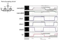
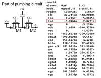
I am doing charge pump for white LED now.
The output current is around 60mA (for the three white LEDs in parallel)
I checked the two power PMOS, and I found out that there's a 5 to 10mA current
that flows from drain to bulk (Ibd).
How can avoid this? or is there any technique to minimize it?

61_1289518956_thumb.jpg
[/url]

Thank you..
 

Is your drain voltage swinging to above the N-well (or N-bulk)?

5mA reverse leakage would mean either the model's whacked
or the device is way overstressed.
 
hello dick_freebird..
From the A-waves below, I supposed the drain voltage is swinging higher than the n-well.
The bulk of the two PMOS is connected to the Vdd (or Vin ) here.

As we can observe, the current is swing has positive and negative magnitudes.
As PMOS, I believe that the current would only have negative magnitudes.
But here, drain sometimes becomes higher than the source, which makes the appearance
of positive magnitudes for the current.
Please correct me, if I'm wrong with this.

My other concern also is in this architecture, the two bulks of the two PMOS are connected.
I'm afraid, there's a problem that would arise.

44_1289525383_thumb.jpg
[/url]

Thank you.
 
Status
Not open for further replies.

Similar threads

Part and Inventory Search

Welcome to EDABoard.com

Sponsor

Back
Top