Continue to Site

Welcome to EDAboard.com

Welcome to our site! EDAboard.com is an international Electronics Discussion Forum focused on EDA software, circuits, schematics, books, theory, papers, asic, pld, 8051, DSP, Network, RF, Analog Design, PCB, Service Manuals... and a whole lot more! To participate you need to register. Registration is free. Click here to register now.

Doubts on Allegro PCB editor

Status
Not open for further replies.

Deepikaaa

Member level 2
Joined
Mar 17, 2011
Messages
43
Helped
23
Reputation
48
Reaction score
22
Trophy points
1,288
Location
Chennai, Bangalore
Activity points
1,527
Hi frnds....

I am having some doubts on allegro pcb editor... I thank u so much for you reply..

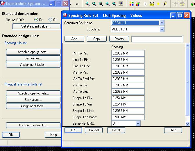
1. I want to know that what are the necessary values to be set in the constraint manager??

2. how to make holes in the four corners of the board??

3. How to make holes in the base of one of the IC pad-stack to be used as a soldering hole??

Thank u so much...

Deepikaa
 

assume you are new to PCB design
1 . constraint manager - depends on your PCB reqiurement. It may be physical clearance to SI constarints like lenghth matching, cross talk,impedance etc
2. Mounting holes -- location and drill size - depends on enclosure/casing/cabinet whre PCB is spoosed to rest
can be placed as symbols in allegro
3. means Thru hole component?? Use padstack designer
 
yea... s sir.. i am a beginner to this allegro.. thank u so much for your response and also for spending your time for me.
can you plz say me that what are the parameters should be set in the physical, electrical and spacing constraints??

Deepikaa
 
for normal designs setting spacing parameters,select via from physical etc will do

 
thank u sir...

can u plz say me that where is mounting hole option???
and also i want to put some holes in the one of the padstack of IC, which is to be used as an soldering hole.. my hardware engg told me that the ic is having ground pin on the base of the IC.

Deeps....
 
for mounting hole you may need to crate new DRA file with desired drill size. Some footprints are available at

<installed locations>:\Cadence\SPB_15.7\share\pcb\pcb_lib\symbols\

regarding the IC I am little bit confused are you looking for a thru hole IC( DIP IC) .

Normally packages like QFN comes with a pad .In picture Pin 25 . But here we need a SMD pad for soldering and manually such soldering is difficult and need to go for machine soldering.

12_1300357035.jpg
 
sir..

that is SMD IC, which s having 25th pin on the bottom base.. i need to put a hole for two purpose. the major reason is to hold the IC firmly....
what kind of hole i can use..via?? how to assign?? plz guide me sir..

Deepsss..
 
Hi Deepsss,

I think you have multiple options here.

1 . Place a Via with required size
2. Place a symbol ( just like you added mounting hole)
3. In the footprint itself define a thru hole pad ( ie for the last picture the 25th pin will be a thru hole pad , you can place it as a 'mechanical pin' if you dont need any connection there. or defie it as a 'connect pin' and in your schematic symbol there will be 25 pins.

And I believe the best option is the 3rd one.
 
Last edited:
Status
Not open for further replies.

Part and Inventory Search

Welcome to EDABoard.com

Sponsor

Back
Top