dirac16
Member level 5
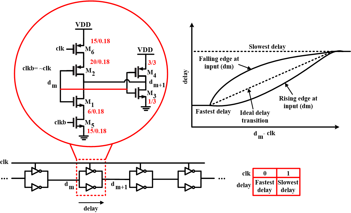
I have a double-delay inverter chain as shown in the image. The actual purpose of this inverter chain does not matter for the sake of this question. Each double-delay inverter is formed by parallelizing two small and large inverters. The small inverter can be turned off by a gating control signal clk as shown. When clk=0 (and clkb=1) the small inverter is on and its parallel connection with the large inverter (formed by M3 and M4) makes a small delay inverter. When clk=1 (and clkb=0) the small inverter is turned off and the delay becomes the delay of the large inverter. That is how it works.

There is something I cannot understand though. According to my simulations, the actual delay transition from fast to slow does not change linearly. In other words, the delay is observed to be non-linear and for the given double-delay inverter it further depends on whether the input at the instance clk rises is rising or falling. Where does that non-linearity come from? I would guess it might be due to the different turn-off times of the gating transistors M5 and M6. But they have equal sizing as shown and it may not be the reason. So what actually do you think that might be the cause? I have been stuck for days trying to understand this but no success.
There is something I cannot understand though. According to my simulations, the actual delay transition from fast to slow does not change linearly. In other words, the delay is observed to be non-linear and for the given double-delay inverter it further depends on whether the input at the instance clk rises is rising or falling. Where does that non-linearity come from? I would guess it might be due to the different turn-off times of the gating transistors M5 and M6. But they have equal sizing as shown and it may not be the reason. So what actually do you think that might be the cause? I have been stuck for days trying to understand this but no success.