Continue to Site

Welcome to EDAboard.com

Welcome to our site! EDAboard.com is an international Electronics Discussion Forum focused on EDA software, circuits, schematics, books, theory, papers, asic, pld, 8051, DSP, Network, RF, Analog Design, PCB, Service Manuals... and a whole lot more! To participate you need to register. Registration is free. Click here to register now.

Discrete MOSFET bias using datasheet

Status
Not open for further replies.

AlienCircuits

Member level 5
Joined
Jun 14, 2012
Messages
81
Helped
0
Reputation
0
Reaction score
0
Trophy points
1,286
Activity points
2,134
Hello,

After careful review of my book Sedra and Smith, I see that in almost all of his designs he references the process parameters K = k'n*(W/L) which has units of mA/V^2.

My problem now (as it was when I first studied it) is that there is a disconnect between what this book teaches and what a MOSFET datasheet provides. I'm hoping someone can clarify this for me.

My MOSFET datasheet only gives me a transconductance parameter g_fs, however this is in units of A/V, so I know that I cannot use the equations Sedra and Smith use with this parameter. I want to use these equations to determine my bias current for saturation operation, iD = K*(Vgs-Vth)^2.

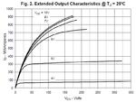
I have asked this question before a long time ago and I never got an answer that actually helped me resolve this issue to where I could start designing FETs as amplifiers with real parts. Without knowing more, the only way I can guess to figure out K would be to try and derive it graphically from the Id - Vds plot of various Vgs curves.
 

Did you check: https://en.wikipedia.org/wiki/MOSFET? look below "Saturation or active mode" and especially the last part above "body effect".

The simple square law models doesn't take higher order effects into account that become dominant at higher current density.

A search on: mosfet model velocity saturation, will give you useful information (I used google).
 
Last edited:
After careful review of my book Sedra and Smith, I see that in almost all of his designs he references the process parameters K = k'n*(W/L) which has units of mA/V^2.
... and is called transconductance factor, and this is a large-signal parameter.

My problem now (as it was when I first studied it) is that there is a disconnect between what this book teaches and what a MOSFET datasheet provides. I'm hoping someone can clarify this for me.

My MOSFET datasheet only gives me a transconductance parameter g_fs, however this is in units of A/V, so I know that I cannot use the equations Sedra and Smith use with this parameter.
Right. g_fs (or gm) is the (small signal) transconductance parameter which is used for gain calculation at a certain operation point.

I have asked this question before a long time ago and I never got an answer that actually helped me resolve this issue to where I could start designing FETs as amplifiers with real parts. Without knowing more, the only way I can guess to figure out K would be to try and derive it graphically from the Id - Vds plot of various Vgs curves.

Right. From discrete MOSFET datasheets you never get K=µC'ox ; you only can try and derive it from the output characteristic. But in order to fix a certain operation point you can get the necessary Vds, Vgs, Ids values directly from this output characteristic.
 
Did you check: https://en.wikipedia.org/wiki/MOSFET? look below "Saturation or active mode" and especially the last part above "body effect".

The simple square law models doesn't take higher order effects into account that become dominant at higher current density.

A search on: mosfet model velocity saturation, will give you useful information (I used google).

Thank you. I am using 2 MOSFETs. One I am biasing to control the voltage at the gate of another MOSFET, and I am using this MOSFET as a source follower. The biased MOSFET I am using so far can have a large Vds voltage, so perhaps I will have to take into account channel modulation altering my id equation. Both FETs will have very low currents.


... and is called transconductance factor, and this is a large-signal parameter.


Right. g_fs (or gm) is the (small signal) transconductance parameter which is used for gain calculation at a certain operation point.


Right. From discrete MOSFET datasheets you never get K=µC'ox ; you only can try and derive it from the output characteristic. But in order to fix a certain operation point you can get the necessary Vds, Vgs, Ids values directly from this output characteristic.

I notice in the book that the large signal transconductance factor and the small signal transconductance parameter seem to be related because the factor is a constant when taking the derivative to get the small signal "linear" gain. When you say output characteristic do you mean the iD vs. Vds plot with Vgs curves?
 

..... Yes!

Hmm.. then I may be in trouble!

My output characteristic curves only go down to about 50 mA, and I want to bias this FET at about 150uA.

outputcharacteristics.png

I have been able to get a biased circuit using this FET spice model to work in simulation.

I add a source degenerative resistor and am able to vary my Vgs from 2.98V to about 3.05V by varying the gate voltage from 3.03V to 14.7V. My resistors are picked from rough calculations/guesses and I wanted to bias it "properly" by doing it by the book to verify that my values are appropriate.

My instincts tell me to be worried by the fact that my Vgs varies so little (I have read about subthreshold operation, and I wonder if this could count as that) and that my bias current is so low. My PSPICE simulation seems to say everything is alright though, so I'm not sure if I'm headed down a road of disaster or not.

Also, please take the above as one post and if anyone has anything helpful to say about it, I always appreciate that. I just wanted to add this tho:
Even with a 1200V part, I still had to add a shunt resistor (in parallel with the leakage current of the FET) to protect my FET when it was turned off at the worst condition because Vds was breakingdown and conducting almost like a zener in my PSPICE simulation (i assume in real life that it would die). So, anyway, the reason my output characteristics only goes down to 50mA is because I had to use a 1200V part because of the very high input voltage condition. If I can use a shunt resistor and pick a less high rated Vds part, I might be able to get a better small signal application FET and still protect it with a shunt resistor.
 
Last edited:

What are you trying to measure, make, design, etc?

Your datasheet may have a graph showing Id versus Vgs at constant Vds (often at two or three temperatures). Does this give you data at lower current?
 
What are you trying to measure, make, design, etc?

Your datasheet may have a graph showing Id versus Vgs at constant Vds (often at two or three temperatures). Does this give you data at lower current?

I am trying to design a high voltage regulator. Basic specs are like this: 1600V to 1000V input voltage, 800V output voltage, 5mA max input current, 0-500uA output current (will probably actually only draw 300uA max). My initial design was to use a buck regulator, and then someone here (it might have been you even) told me that it would be much simpler to design a linear regulator since the power drop across the regulated component would be so low. I have decided to try to make a series pass regulator, and so I must control the gate voltage of my pass element. I chose the MOSFET that I did because it is rated for 1200V and has only 1uA leakage current.

The plot that I provided is the graph with the highest resolution at low currents. It does have more plots tho:
**broken link removed**
 

My output characteristic curves only go down to about 50 mA, and I want to bias this FET at about 150uA.

I have been able to get a biased circuit using this FET spice model to work in simulation.

With this spice model you should be able to plot the (for you) interesting range of the output characteristic, see e.g. the image in this thread (left bottom clipping from the output characteristic on the right).

Anyway; don't forget that threshold voltages and so the output curves are temperature dependent.
 
About transconductance at low current:

Graph 7 shows the Id versus Vgs curve. To get mA range drain curent, Vgs will be around 3V. Figure 8 shows the transconductance. At low drain current it is proportional wtih current (so you are in the quadratic region of mosfet operation). From the graph, it is the range of 4 mA/V/mA (4mS/mA). IXYS doesn't show DC safe operating area, but with this low current this should be OK, provided that you can avoid the inrush current for the regulator in case of large capacitive loads.

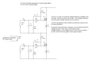
With one device, you cannot accept 1600V supply in case of a series circuit regulator, as your output voltage starts from zero. I would not rely on avalanche caracteristics without rigorous testing. You need to stack at least two of the HV mosfets. You may consider a topology as shown below:

 
Just thought I'd let anyone know what has come of this. I have built the simple series pass circuit and it takes 1600V in and puts out 800V (i can change this with a potentiometer of course). It works pretty well, and now I'm designing a voltage regulator from it. I have a crop of new issues to ask about though.

Also, I was able to obtain Vgs output curves of Id vs. Vd as low as a few microamps from the spice model.
 

A few things -

- A power FET meant for amps probably has a poorly
spec'd, modeled and controlled leakage floor.

- A VDMOS or LDMOS device is unlike a plain MOSFET,
it resembles more a MOSFET with a cascode JFET at
the drain. Its transition from linear to saturation will
likely occur at lower drain voltage than you'd expect
from MOS theory and need extra work, have extra
error if you try to fit it with a single MOS model

- DMOS devices don't always like being run linear.
Power is highly concentrated in the necks and you
may not find the derating info you need for a linear
application of a "switching" type device.

- If you depend on cascodes for device survivability
you are depending on leakage balance at high voltage,
another thing that is poorly modeled if at all. A minimum
pass-stack current (minimum load current) is a good
idea; at some point of low current the cascode may
fail to prevent overvoltage if it leaks too much for
the setpoint of the master device.
 
Did you only use one mosfet or a stack of two of them?

Just 1 MOSFET.

schematic: View attachment hvps2.pdf

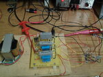
prototype: hvps.jpg

One of my FETs keeps failing and I'm trying to get to the bottom of it right now. It is the first series pass FET in the schematic I attached. I have built a 2 stage version of this regulator and I have been having success at regulating 800V out. I feed my design with a rectified input from a transformer that takes line voltage of 115Vrms and steps it up to 1000Vrms (1414V peak). I am using a variac to control the line voltage from about 80V to 140V and it still works as I vary the input with no transient overshoot or undershoots.

The way I have been getting my FETs to fail is to bring the variac to the low end, at 80V in, and then sweeping it to >115 as quickly as my hand can turn it after the circuit has been already running fine for a few minutes. Once I do this, my series pass FET "shorts" out and my first stage regulation is ruined until I replace the FET. I've tried substituting a 1500Vds, higher current rated, FET too and the same problem happens (they actually fail more often). When I measure the drain to source resistance of these failed parts I get 1.2kohm and gate to drain resistance is 3.2kohm, which is not a short but much lower than I should get.

Also, the transformer is not my choice, and my circuit has to work with it. Once I have this circuit working, I'd like to replace the transformer with a boost converter.
 
Last edited:

The design concept sounds unrealistic. You won't be able to operate a discrete FET at a defined current by just a specific Vgs. Any real circuit would use current controlled feedback to achieve this.
 

The design concept sounds unrealistic. You won't be able to operate a discrete FET at a defined current by just a specific Vgs. Any real circuit would use current controlled feedback to achieve this.

I am just trying to control the output voltage though, the current is not defined. The load current will most often be less than the current in my feedback paths, and it would never go above 500uA probably. My simulations show that it can source 1mA pulsed or DC at 800V just fine though. I just was testing the circuit with a current source as a load.
 

There is a time constant of 25ms in the first control path. May be it's too large for your variac manipulation.

In any case I'd put a Z-Diode between gate & source of your pass-FETs; perhaps this may save you some of them.
 
In any case I'd put a Z-Diode between gate & source of your pass-FETs; perhaps this may save you some of them.
I didn't previously notice the circuit diagram. Potentially applying high gate voltages without safe clamping is an absolute No-No and the fast track to ruin the transistor. Drain-source overvoltage with low energy will be in contrast absorbed by it's avalanche capability.
 
I didn't previously notice the circuit diagram. Potentially applying high gate voltages without safe clamping is an absolute No-No and the fast track to ruin the transistor. Drain-source overvoltage with low energy will be in contrast absorbed by it's avalanche capability.

I remember I had a zener on my gate to source junction very early on in the design, but I took it out for simulation at some point. I thought this would not be an issue since the FET is supposed to be a source follower where the Vgs should never exceed the limit. I guess when the input changes very fast, the gate and source voltage could come out of phase with the junction capacitances and exceed the Vgs for some time. I just looked at the Vgs in my simulation and see that there is a 50V spike at start up.

As soon as I get more FETs I'll add the zener for protection and test it out.
 

Status
Not open for further replies.

Similar threads

Part and Inventory Search

Welcome to EDABoard.com

Sponsor

Back
Top