Continue to Site

Welcome to EDAboard.com

Welcome to our site! EDAboard.com is an international Electronics Discussion Forum focused on EDA software, circuits, schematics, books, theory, papers, asic, pld, 8051, DSP, Network, RF, Analog Design, PCB, Service Manuals... and a whole lot more! To participate you need to register. Registration is free. Click here to register now.

Dimmable Ballast for Fluorescent Lamp

Status
Not open for further replies.

jp1016

Newbie level 4
Joined
May 20, 2013
Messages
6
Helped
0
Reputation
0
Reaction score
0
Trophy points
1,281
Activity points
1,390
I'm new to the forum, so Hello World! Of course I have registered here because I need help with something, but the forums topics seem quite interesting, so I believe I'm about to become a follower.

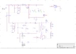
Here's the deal: I have designed for my final work at college a dimmable ballast for a fluorescent lamp. The power circuit is as seen on the attached picture. It is composed basically of an LC input filter, of a full-bridge rectifier, a PFC-Boost stage integrated with a half-bridge inverter stage, and a resonant LCC filter on the output. The Lamp is represented by the equivalente steady-state resistance, derived from the voltage and power data informed by the manufacturer, that is, 101 V and 39W. The switches are turned on alternately, with a frequency that varies from 45 to 80 KHz, and a duty cycle that varies from 0,43 to 0,31, according to the desired output power (100% to about 30%). The capacitors C2 and C3 were calculated so that their voltage stabilizes at around 325 V, so the LCC tank receives a pulsed voltage of 325 V of amplitude, and filters it so that a sinusoidal voltage of 101 V (rated condition) is applied to the lamp. I have simulated the circuit thoroughly with PSpice and PSIM, and obtained the expected results. However, when I turn my prototype on on full power, it lights up the light, which keeps on for a while (30 seconds, maybe), until the MOSFET M3 burns and a short path is created from its Drain to its Source.
I have very little practical experience with electronics and circuit design, but I need to get it working within the next 15 days, otherwise I might have problems graduating =D Do any of you have a clue of what might be going on with my switch? I have replaced it and it burned again, and the last time I realized that the MOSFETs heatsink was quite hot. I've thought of buying a bigger heatsink, but I don't suppose that overheating should be a problem, given that the MOSFET (2SK1120) is rated for 150W power dissipation, and [I think that] power losses on the switch shouldn't be higher than some 5W.

Any thoughts? Thanks in advance!

image.png
Prototype.png
 

"a PFC-Boost stage"

One does such a stage for power factor correction. To do so, the waveform drive is dynamically adjusted.
But your schematic that you show is absolutely incomplete. It cannot be a steady state pulse

What IC are you using to drive M3, what are its passive component values, what are your calculations you made to reach those values, what is the saturation current of the inductor? Are you really using a plain vanilla rectifier for the boost rectifier? What mode of operation have you chosen, continuous, discontinuous or critical?
 

I think you're misusing the terms PFC and LLC, I don't see either in the schematic. I can't really see the operating principle of the circuit, especially M4. It looks like the "boost" stage is just going to send tons of ripple current into C2 and C3.
 

Ok, so, first of all, thanks for your answers.

Indeed, I think I have skipped information. Attached you will find a more complete picture of my circuit (I have changed the names of some of the components, so that referencing them is easier - the 1T resistors are only to aid convergence). The structure of this circuit was not conceived by me, as you can already deduce out of my lack of experience with power MOSFETs. It has been presented by a brazilian engineer on a masters degree paper, along with all equations to calculate the main components. However, some of the most peripheral components (voltage sources and control circuit) were not the issue os his paper, and since I lack practical experience, I'm having trouble getting it to work. I do, however, get the theoretical idea of his work, which I will describe below.

Circuito.xps.1.png

The circuit does not properly contain a PFC-Boost converter, but rather a Buck-Boost converter, composed by DBoost, LBoost and M3, operating in a way that the voltage gain is bigger than one (just like a Boost Converter). I have called it a boost converter because its function is similar to that of the PFC-Boost converter normally seen on Fluorescent Lamp Ballast circuits. It operates in discontinuous mode, but since there is no capacitor after the rectifier stage, the voltage applied to the inductor is the modulus of the sinusoidal network voltage, and the current on the inductor has a quasi sinusoidal overall shape. The low-pass LC input filter composed by both Lf and Cf grants that only the low frequency current drawn by the circuit is seen by the AC source, as you can see on the attached picture hereunder (now simulated with PSIM - I now realize that PSpice is generating a source current with and angle of close to 90° in reference to the voltage - there must be something wrong with the real-world values I used for my components, since PSIM uses ideal models).

VAC-IAC -- VACfilter-IACfilter.png

The LCC filter is composed by Cs (56nF), Ls (2.88mH) and Cp (5nF - two series 10nF/1600V were used in the prototype because during transient, voltage spikes of up to 1500V might hit the lamp, and I thought: "Hell! Why not oversize it?").

There are four operation steps on this circuit:
1) The first step starts when M3 starts to conduct in Zero Voltage Switching Mode, since its intrinsic diode was already conducting on the reverse direction on the 4th step of the last period. IBoost rises linearly, while the capacitor C1 discharges, with its current flowing through the LCC circuit and powering the lamp. The voltage and the current on the lamp both rise.
2) Starts in the moment M3 is blocked. IBoost starts to fall linearly, charging the capacitors C1 and C2. The energy stored in the Ls inductor in the last step discharges as current through the intrinsic diode of M4, and through the load. Voltage and current on the load both fall linearly. M4 is enabled to conduct during this step.
3) This step starts in the moment the current through the intrinsic diode of M4 becomes null, and M4, which was already enabled, starts to conduct in ZVS the current of the capacitor C2, which now discharges over the load. Voltage and current on the lamp rise linearly, with reverse polarity to that of the first step.
4) Starts when M4 is blocked. The energy stored in Ls discharges as current flowing through the intrinsic diode of M3. IBoost starts to rise while charging the capacitors C1 and C2. M3 is enabled to conduct. The voltage and current on the lamp falls linearly, also with reverse polarity to that of the second step.

You can see the resulting simulation curves in the attached image, with emphasis on the operation steps:
curves.png

As for the control signal, it is generated by the PWM of a microcontroller (PIC18F4550 - represented by the pulsed voltage sources), and that signal is galvanically isolated from the power circuit by a pair of pulse transformers. The circuit I have attached also includes the auxiliary DC sources to provide 15VDC to power the MOSFETs gate and the 5 VDC to power the microcontroller (there is also a 3.3VDC voltage regulator cascaded with the 5 VDC one for a zigbee module, but I don't think that it is relevant to this current problem I'm having).

Ok, now that I have introduced you to what I'm trying to do, back to my query. I believe my real problem is actually related to this last paragraph I wrote above. More specifically, with my 15V supply. It doesn't produce 15 V :D ...but only about 6~7 VDC (I have measured that with a multimeter). I think that it happens because the impedance of the pulse transformer (3mH + 0.76R) is much lower than that of the zener diodes, so no current flows through them when Q2 or Q3 are on, bringing the voltage on the 15V bus to a value close to zero, and implying in and average value of around 6 V, as described.
I have been thinking of this problem the whole day, and I have come to the conclusion that my MOSFET is not operating on the saturation region, because VGS on the switches is equal to +6 VDC when on, and equal to -6 when off - way less than the minimum rated 10V. Could you guys please confirm that the symptoms I described, that is, overheating and eventually burning, agree with this diagnose? And if, in fact, what I suspect is right, could you suggest a better structure to provide 15V that would not cause the same problem?

Thank you again in advance!
 

First of all, thank you for a very thorough explanation.

I believe that your suspicions are correct, that the auxiliary bias supply is not capable of producing the required voltage or current, and therefore your Mosfets are not being driven properly. That the is Mosfet overheating is a good clue to that.

I would use the "divide-and-conquer" approach to solve your issue. Divide your circuits in smaller subassemblies and conquer its problems individually.
What I would do first, is to replace the auxiliary supply with a tried and true circuit...i.e. one having a 220/18V 250 mA transformer, feeding a bridge rectifier and capacitor, and regulated by a 7815 regulator.

Another thing you may want to replace is the plain vainilla 1N5404 in the "boost" circuit with a fast recovery diode like UF5404.
 

Well, I understand that it is more certain to work with a transformer, but couldn't I just keep the 1.5uF capacitors from the AC to the rectifier bridge, followed by a 20V zener in series with a resistor, and in parallel with the zener, the LM7815? (I'm on lunch at work and have no access to a spice program to provide a schematic)

As for the diodes, actually I'm using 1N5408's, which I haven't found on PSpice, and which I suppose are even worse, because they are rated for a higher voltage, and their recovery time must be even bigger. I intend to accept your suggestion and replace the ones on my circuit.

Thank you once again!

- - - Updated - - -

Just realized another mistake by my part. My DBoost is actually an UF4007. I have mistakenly represented it with an 1n5404. When you were speaking of the boost diode, I was for some weird reason thinking of the rectifier bridge diodes.
 

"Well, I understand that it is more certain to work with a transformer, but couldn't I just keep the 1.5uF capacitors from the AC to the rectifier bridge, followed by a 20V zener in series with a resistor, and in parallel with the zener, the LM7815?"

Yes you may do that...but after you have properly debugged the main powertrain. That this section operates without failures and within your performance constraints.

Remember: divide and conquer.

With respect to the UF4007, this is a good fast diode, but older technology. Its recovery time characteristics may cause significant ringing, and you may be required to add some snubbers...do you have access to a scope?
 
  • Like
Reactions: jp1016

    jp1016

    Points: 2
    Helpful Answer Positive Rating
Okay I get the operation of the converter circuit, thanks for the explanation.

The gate drive circuitry looks pretty buggy. Even besides the issues with transformerless power supplies, the way you use those two NPN BJTs to apply the pulses on the primary can't work well. Are you sure you didn't mix up the emitters and collectors there? Also you probably want to reverse diodes D15 and D18, to avoid cross conduction (rather than encouraging it).

And if you actually built the circuit using the transformerless power supply, then debugging it is going to be very difficult (unless you have good isolated probes). If it were me I would use an isolated bench supply for the control and gate drive, and have the AC line isolated (and use a variac as well). Then you can earth various nodes to probe them in relative safety.
 

Well, ok... Transformer bought! I will try a few things and tell you how it works out. I do have a lent portable oscilloscope with me, but its downside is that it has only one channel, which is a real pain in the ass for some things.

mtwieg, you're right about mixing the emmiters and collectors of the BJTs, but I only did it on PSpice when drawing the circuit to explain it to you guys. On my prototype, the BJTs are set right. However, regarding the diodes, I now owe you some real gratitude. I had been working all along with the diodes the wrong way around. To be honest, I think I haven't fully understood their function in that particular circuit.
 

After fifteen days breaking my head to find out what was wrong with my circuit, I come to see that it was not only on the spice schematics that my BJT was inverted -.- And believe me, I had checked it more than once once... That was rather frustrating....
 

Glad that you could find the problem....

Yes, those kind of things happen, even to seasoned veterans.......part of a learning process.
 

Not surprising it's something like that. Does the circuit work okay now?
 

Well, sorry, I forgot to check back on this thread after I found out what the problem was. Yes, the circuit worked, but then I found out I had thermal problems. My dimmable ballast only worked with forced cooling. Otherwise, the Mosfet would always burn after a few secs. I didn't know until then that MOSFETs were not the ideal switches for over 500V of blocking voltage. In my circuit, I had about 700~850 V between Source and Drain, and at that voltage level, the RDSon resistance was way too high, causing constant heating, and bringing the converter efficiency to a very low level.
 

Status
Not open for further replies.

Similar threads

Part and Inventory Search

Welcome to EDABoard.com

Sponsor

Back
Top