Continue to Site

Welcome to EDAboard.com

Welcome to our site! EDAboard.com is an international Electronics Discussion Forum focused on EDA software, circuits, schematics, books, theory, papers, asic, pld, 8051, DSP, Network, RF, Analog Design, PCB, Service Manuals... and a whole lot more! To participate you need to register. Registration is free. Click here to register now.

Diiference between D-MOSFET and V-MOSFET?

Status
Not open for further replies.

graciousparul

Full Member level 2
Joined
Jan 19, 2008
Messages
128
Helped
6
Reputation
12
Reaction score
0
Trophy points
1,296
Activity points
2,053
hello


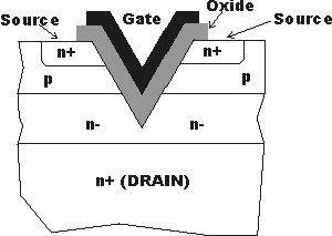
What's the difference between D-MOSFET and V-MOSFET?

and also tell me which is the good refrence book for high power devices other than Baliga?

Thanks for ur help.
 

Hello
Just did a paper on this recently. Here is a copy from my paper minus the quotes.
VMOS field effect transistors or FETs are a form of power MOSFET and these electronics components are used for a variety of applications where medium powers are required. The VMOS FET gains its name from the fact that it is "Vertical Metal Oxide Silicon". From this it can be imagined that the VMOS FET has many similarities to MOS technology, but the structure is arranged with a V-groove which also adds another dimension to the name VMOS.
When VMOS FETs were first introduced they out-performed bipolar semiconductor technology in many respects making the design of amplifiers much cheaper and easier. Since their introduction VMOS FETs have become firmly established as useful power MOSFET electronics components that can be used for a variety of power MOS applications ranging from power supply switching applications through to medium power RF amplifiers. They are also incorporated into many integrated circuits as they are able to switch very quickly. MOS FET structure
VMOS FETs are able to overcome many of the problems which prevented FETs being used in power applications. Their new structure enabled much higher powers to be handled than was previously possible with bipolar transistors of an equivalent size and cost.
The reason for this great improvement lies in the structure of the device. To show the advantages of a VMOS FET a traditional MOS device. Here it can be seen that the drain and source are separated by the gate. Current flows horizontally between the source and drain, controlled by the potential on the gate. As the current only flows through a relatively small area, resistance values can be high reducing the efficiency of the device.
The VMOS FET uses a different structure. The most striking point about the new device is the V groove in the structure which is the key to the operation of the device. It can be seen that the source is at the top of the device, and the drain is at the bottom. Instead of flowing horizontally as in the standard FET, current in this device flows vertically giving the device its name - Vertical Metal Oxide Silicon, VMOS.

VMOS field effect transistor structure
The device uses two connections for the source and accordingly there is a much large area through which the current can flow. This reduces the ON resistance of the device allowing it to handle much higher powers than conventional FETs.
The gate consists of a metallised area over the V groove and this controls the current flow in the P region. As the gate is fabricated in this way it means that the device retains the exceptionally high input resistance typical of the MOS family of devices.
The main drawback of the VMOS FET is that the structure is more complicated than a traditional FET and this makes it slightly more expensive.
28_1303511345.jpg


---------- Post added at 23:34 ---------- Previous post was at 23:30 ----------

As far as getting information on Hi power devices web searches are my best choice.
 
yes MONTECH, I agree with you completely ,i have found harldy two differences only .
 

Status
Not open for further replies.

Similar threads

Part and Inventory Search

Welcome to EDABoard.com

Sponsor

Back
Top