Khazan
Junior Member level 1
Hello experts:
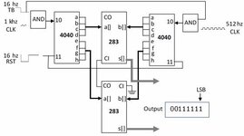
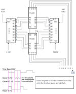
As the attached schematic shows, I am experimenting a circuit for adding two numbers represented by two digital counters and two cascaded 4 bits adders (74hc283). I tested separately with cascaded 74hc163 and with asynchronous 74hc4040 counters and I ended up with the same questions.
I fee one of the counters (at pin 10) with a 1 khz clk signals and the second counter with 512 hz signals. All signals are well formed square signals.
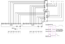
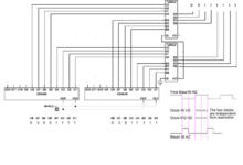
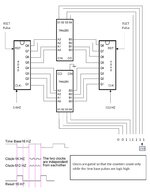
I use 16hz crystal-controlled time base. The counters count during logic high of the time base that is 1/32 sec or about 31 msec. The counters are reset (at pin 11) in the second half of the logic-low of the time base.
When I verify the outputs of the first counter, my prob realizes pulses at some of the outputs and I consider them as logic high. So that the output of the first counter is binary 00011111 to represent the 1khz clk input, almost as expected. The output of the second counter is binary 00001111 to represent the 512 hz clk input also during the 1/32 sec. So far so good.
I feed input a[] of the cascaded adders by the outputs of the first counter and input b[] of the adders by outputs of the second counter. My expectation is to see the correct sum as binary number 00101110 at output s[] of the 8 bits adder, the same way that I see the correct binary numbers at the outputs of the two counters. But instead, I see binary 00111111 as the sum. If I change the clk input of the first counter to 2khz and I leave the clk input of the second counter as it was 512 hz, I see binary number 01111111 instead of the correct sum 01001110 as sum at outputs s[] of the adder. If I change the clk input of the first counter to 512khz like the second counter, I see the correct output of 00011110 as sum at outputs s[] of the adder.
Is my expectation to see the correct sum at output s[] of the adder justified while the counters are counting during the logic high of the time base?
If so, why do I get wrong sum?
If my expectation is wrong then how am I supposed to get the right sum while the counters are counting during the logic high of the time base?
Please note that it is not about what kind of counters I am using. It is about the wrong sum no matter which counter I use.
Thank you
As the attached schematic shows, I am experimenting a circuit for adding two numbers represented by two digital counters and two cascaded 4 bits adders (74hc283). I tested separately with cascaded 74hc163 and with asynchronous 74hc4040 counters and I ended up with the same questions.
I fee one of the counters (at pin 10) with a 1 khz clk signals and the second counter with 512 hz signals. All signals are well formed square signals.
I use 16hz crystal-controlled time base. The counters count during logic high of the time base that is 1/32 sec or about 31 msec. The counters are reset (at pin 11) in the second half of the logic-low of the time base.
When I verify the outputs of the first counter, my prob realizes pulses at some of the outputs and I consider them as logic high. So that the output of the first counter is binary 00011111 to represent the 1khz clk input, almost as expected. The output of the second counter is binary 00001111 to represent the 512 hz clk input also during the 1/32 sec. So far so good.
I feed input a[] of the cascaded adders by the outputs of the first counter and input b[] of the adders by outputs of the second counter. My expectation is to see the correct sum as binary number 00101110 at output s[] of the 8 bits adder, the same way that I see the correct binary numbers at the outputs of the two counters. But instead, I see binary 00111111 as the sum. If I change the clk input of the first counter to 2khz and I leave the clk input of the second counter as it was 512 hz, I see binary number 01111111 instead of the correct sum 01001110 as sum at outputs s[] of the adder. If I change the clk input of the first counter to 512khz like the second counter, I see the correct output of 00011110 as sum at outputs s[] of the adder.
Is my expectation to see the correct sum at output s[] of the adder justified while the counters are counting during the logic high of the time base?
If so, why do I get wrong sum?
If my expectation is wrong then how am I supposed to get the right sum while the counters are counting during the logic high of the time base?
Please note that it is not about what kind of counters I am using. It is about the wrong sum no matter which counter I use.
Thank you