Continue to Site

Welcome to EDAboard.com

Welcome to our site! EDAboard.com is an international Electronics Discussion Forum focused on EDA software, circuits, schematics, books, theory, papers, asic, pld, 8051, DSP, Network, RF, Analog Design, PCB, Service Manuals... and a whole lot more! To participate you need to register. Registration is free. Click here to register now.

Differential amplifier design in cadence

Status
Not open for further replies.

didaka_dido

Newbie level 1
Joined
Sep 20, 2008
Messages
1
Helped
0
Reputation
0
Reaction score
0
Trophy points
1,281
Activity points
1,288
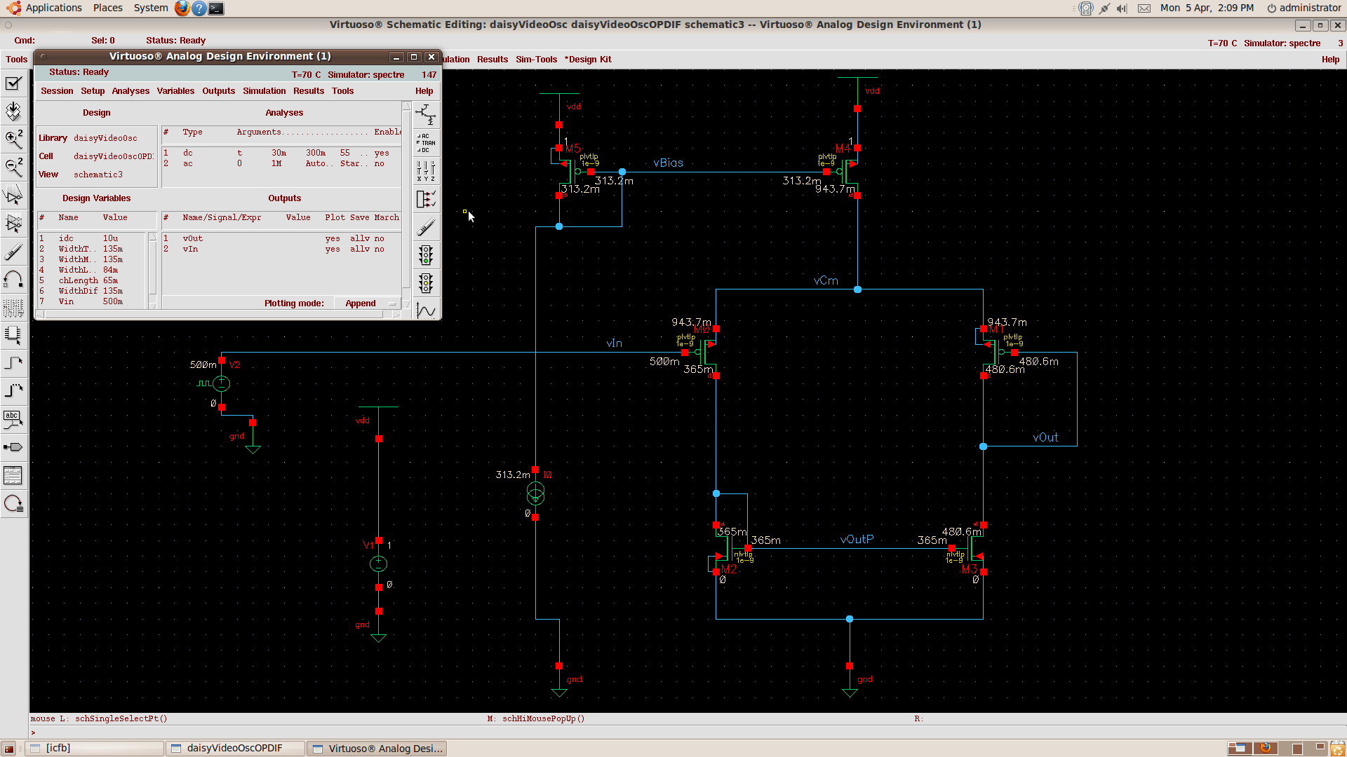
I have a question regarding the design of a differential amplifier with an active load in cadence. My aim is to make it work with supply voltage 1V and current 10~20uA with STM065nm technology. I have problem swinging and getting the right values for the transistor widths. What should be my approach when designing the differential amplifier? Should I start swinging the differential pair or the active load transistor pair first? I managed to achieve a transfer function somehow close to the ideal, but still it is far from the normal one. You can find a screenshot of my schematic below.


Status
Not open for further replies.

Part and Inventory Search

Welcome to EDABoard.com

Sponsor

Back
Top