Continue to Site

Welcome to EDAboard.com

Welcome to our site! EDAboard.com is an international Electronics Discussion Forum focused on EDA software, circuits, schematics, books, theory, papers, asic, pld, 8051, DSP, Network, RF, Analog Design, PCB, Service Manuals... and a whole lot more! To participate you need to register. Registration is free. Click here to register now.

Differential Amlifier - Differential Input Filter - Stability Analysis

Status
Not open for further replies.

stenzer

Advanced Member level 3
Joined
Oct 1, 2012
Messages
867
Helped
123
Reputation
250
Reaction score
185
Trophy points
1,323
Activity points
8,959
Hi,

I'm simulated a differential amplifier which also includes a differential and a common mode input filter. I performed a stability analysis in LTSpice according to [1]. As can be seen, the corresponding phase of the the open loop response (loop gain) starts at -180°, and has a phase margin of 96° when the magnidude crosses the 0 dB line.
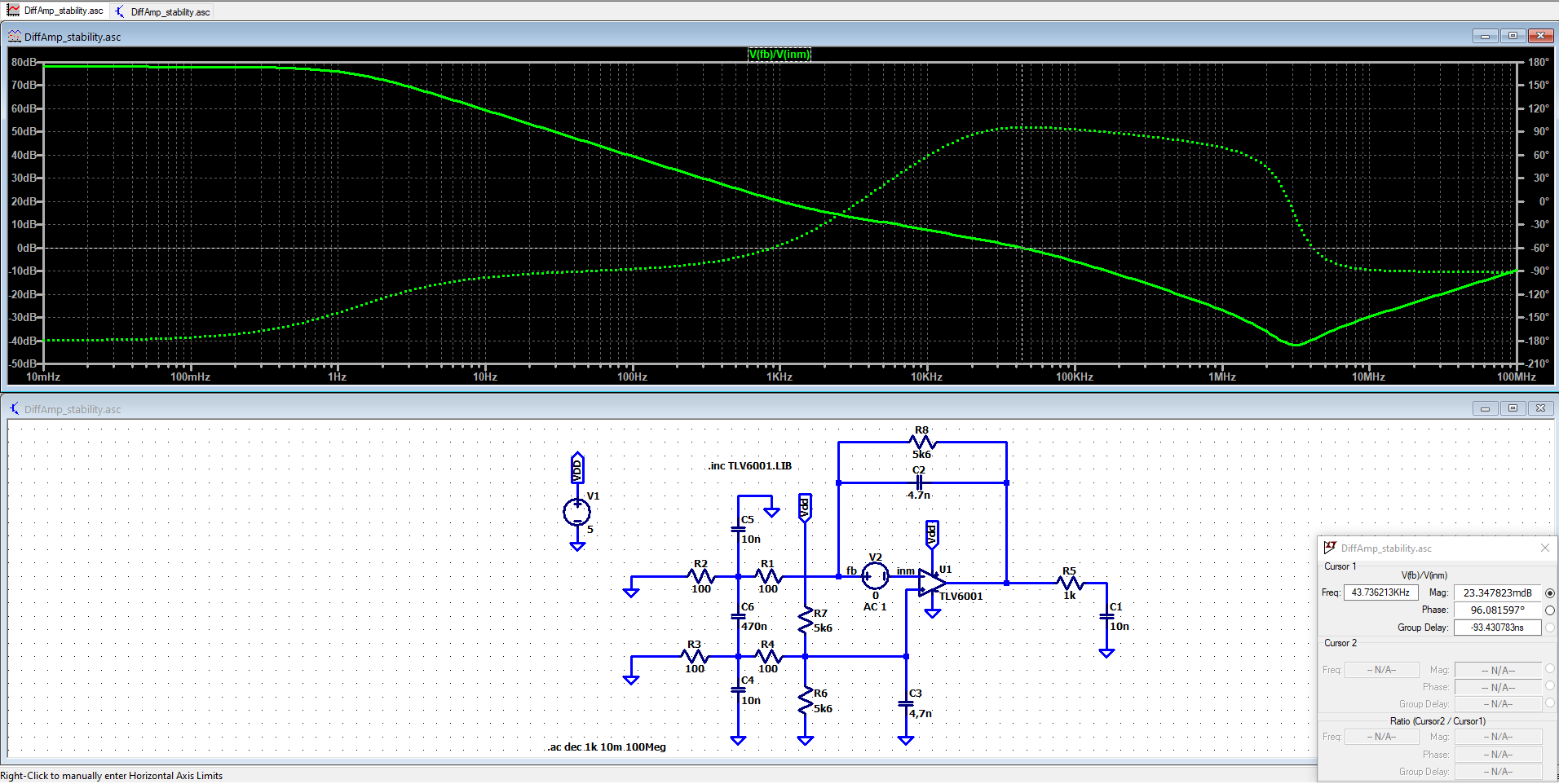
EDAboard_Stability_DiffAmp.png


To consider the circuitry as stable the phase should not be equal -180° for a magnitude of 1 (0 dB) (denominator of the transfere should not be zero ;)), to be more specific a certain phase margin should be maintained.

As the shown circuitry has a phase margin of 96° (@ 0dB) it should be stable. I have performed a couple of stability analysIs in LTSpice so far, but (I think) non started with a phase of -180°. So I wanted to get a feedback from you if my thoughts are correct. Based on my thoughts above, it is only important to have a "large" phase marging (common textbook value is 45°) at a magintude of 0 dB, and to have a small magnitude (<< 0 dB) at -180°.

BR and thank you for your feedback.

[1] https://www.analog.com/en/education/education-library/videos/5579254320001.html
 

You are changing phase of feedback signal by 276 degree, it cannot be stable or testbench is wrong. What is showing step response?
Moreover, the way how you define baseline is tricky. There is a weak voltage divider from vdd to ground (two 5k6 guys) loaded by 200 to ground. And you have a positive feedback because of R1, R4 and C6 path.
BTW Are dc points as expected?
 

Hi Dominik,

attached you can find the step respond result.

EDAboard_Stability_DiffAmp_Step.png


BR
 

Ok. Your DC point are misaligned, so output is very close to VDD, but opamp model seems to be rail to rail.
However, your stability testbench is wrong. Such stuff can work in Spectre simulator which has dedicated stability analysis using Tian method and probe within the loop (analysis is doing all magic itself).
To achieve proper bode plots of feedback signal by exploiting AC simulation, you have to break loop and use at least 3 replicas of circuit to ensure that every point of broken loop can see the same conditions.

The problem with your current testbench is that AC source does not see good ground at any terminal. I know that in some cases is possible to achieve stability results close to real ones, but not in this case.
 

    stenzer

    Points: 2
    Helpful Answer Positive Rating
Hi,

R6 and R7 need to be treated as if they are in parallel. Thus for a true difference amplifier operation each of them needs to be 2 x 5k6 = 11k2

Klaus
 

    stenzer

    Points: 2
    Helpful Answer Positive Rating
Hi,
Ok. Your DC point are misaligned, so output is very close to VDD, but opamp model seems to be rail to rail.
R6 and R7 need to be treated as if they are in parallel. Thus for a true difference amplifier operation each of them needs to be 2 x 5k6 = 11k2

thank you for pointing this out. The DC point is really misaligned, and both of the resistors should be 11k2. This was a "remaining" mistake, as I performed the simulation previously instead of the biasing network only with R6 (R6||R7 --> 5k6). With this adjustment the DC bias is now correct (~2.5 V). The step response shows the same behaviour as shown prevoiusly (with increased magnitude of the voltage step). The open lope AC analyisis is also (almost) identical.

To achieve proper bode plots of feedback signal by exploiting AC simulation, you have to break loop and use at least 3 replicas of circuit to ensure that every point of broken loop can see the same conditions.
Can you please explain this in more detail? I don't get that.

BR
 
Last edited:

Hi,

below the result including the corrected biasing can be seen. The simulation shows the loop gain response starting at 1 mHz up to 100 THz.
EDAboard_Stability_DiffAmp_2nd.png


To get a better picture of what's going on I also created the nyquist plot (locus), shown below. The left plot shows the open loop response, starting from 1 mHz at the left handside and ending at 100 THz, slightly left to the origin (0,0) of the plot. The right plot shows a magnitized version including the unity circle in red, the first pole (starting from low frequency toward higher frequency) marked by a magenta x and the second pole "leaving" the unity circle marked by a black +.

EDAboard_Nyquist.png


By determine the phase margin by the help of the locus, where the phase is evaluated clockwise, starting from the positive part of the abscissa, results in a phase of -264.38° (for the first crossing of the unity circle). Which, is obviously unstabel and alredy indicated in reply #2:
You are changing phase of feedback signal by 276 degree, it cannot be stable or testbench is wrong.
The LTspice result missleaded me, by means of its positive phase sign at 0 db @ 44.5 kHz.

Does some one knows how to evaluate the stabilty of this circuitry in Spice by means of its phase margin? The step response as well as the AC simulation of the closed loop system does not indicate an instability, by means of no overshoothing/peaking.

BR
 

Does some one knows how to evaluate the stabilty of this circuitry in Spice by means of its phase margin?
On this forum is a several threads discussing available methods.
Dominik Przyborowski said:


To achieve proper bode plots of feedback signal by exploiting AC simulation, you have to break loop and use at least 3 replicas of circuit to ensure that every point of broken loop can see the same conditions.

Can you please explain this in more detail? I don't get that.
Quite old method with replica circuits below (sketch is not perfect but didn't took much time):
STB_AC.png

I - closed loop circuit
II - Open loop circuit used to measure closed loop feedback signal - VCVS is sensing feedback net DC to ensure proper bias of open loop replica and VDC with ac=1 is used to provide ac. VFB_OL is measured feedback signal - here you determines phase and magnitude
III - open loop replica ensures proper load for open loop feedback signal
IV - another open loop replica ensures that output stage of replica III has the same DC conditions as I and II - compensates loading effect of III
V - closed loop replica terminating IV.

Not bad approximation you can achieve without IV and V, however it depends to various circuit conditions.
Of course in your case you have to use exactly your circuit - here is only a simple example.
 

    stenzer

    Points: 2
    Helpful Answer Positive Rating
Wow, thank you very much for showing me this approach! I have never seen something like that before.
I will perform an analysis accordingly.

Can you recommend any textbook or articles/app-notes dealing with this kind of analysis or similar techniques, suitable to practical opamp circtits?
I have spent quite a while searching on the web, but I haven't found a "suitable" solution.

BR
 

Can you recommend any textbook or articles/app-notes dealing with this kind of analysis or similar techniques, suitable to practical opamp circtits?
This method has been described by Hurst in one or two papers from ca 1990.

Check also paper from Post number 2 and links from 1st post in linked thread.
 

    stenzer

    Points: 2
    Helpful Answer Positive Rating
Middlebrook's method is applied incorrectly in post #1, because the signal path to the noninverting OP input is ignored.

You can apply the expanded Middlebrook method and get a comfortable phase margin.

1620124838271.png
 

Attachments

  • TLV6001_diffamp.zip
    5.8 KB · Views: 68

    stenzer

    Points: 2
    Helpful Answer Positive Rating
Hi,

first of all thank you all for highlighting methods to performing meaningful stability analysis by SPICE, which I wasn't really aware of.

This method has been described by Hurst in one or two papers from ca 1990.
I assume you mean "Exact Simulation of Feedback Circuit Parameters" by P. J. Hurst [1] (linked to a version provided by P. J. Hurst at his university website at the University of California).

Attached the SIPCE result for the cascaded approche can be seen. I hope I implemented it correct.

- The simulation results in a phase margin of ~106° @ ~33 kHz.
- I also performed a simulation with and without stage IV & V. Therefore, a voltage controlled switch (one iteration ON, second iteration OFF) was used at the entry point of the dashed box of IV. There was no fifference at all, with and without the use of stage IV & V.
EDAboard_Stability_DiffAmp_Cascaded01.png

EDAboard_Stability_DiffAmp_Cascaded02.png


... signal path to the noninverting OP input is ignored.
By mentioning this, I see where my initial error in the initial simulation was made. I only considered the input signal at the inverting opamp input with respect to system ground (GND). But the opamp is changing its output accordingly to the difference between the inverting and non-inverting input i.e. V(inm,inp) in the shown result below. The left circuit and its corresponding trend in green is performed according to [2] (also done in the initial post), resulting in a phase margin of ~106° @ ~51 kHz. The right circuit and its corresponding trend in red is performed according to [3], resulting in a phase margin of ~136° @ ~200 kHz. The green trend results in the same phase margin as the cascaded approach, but at a different frequency (33 kHz vs. 51 kHz). Further, the magnitude of the loop gain of the left circuit (in green) starts to increase for higher frequencies.
EDAboard_Stability_DiffAmp_Compare.png


Now my initial analysis makes more sense, by means of the initial phase shift. The lower two approaches are resulting in plausible phase margins compared to the cascaded approach. Nevertheless, as the cascaded approach is using an unmodified circuitry to provide the biasing of the following replicas, I assume it is the most accurate option.

Regarding the Middlebrooke method:
You can apply the expanded Middlebrook method and get a comfortable phase margin.

Thank you for attaching the simulation. I assume your refernce shown within your simulation comments is "Measurement of loop gain in feedback systems" by R. D. Middlebrook [4]. I will have a closer look at the article, when i find some time (28 pages). Nevertheless, from your attached image, I'm not able to determine the phase margin directly as the evaluated equation is not clear to me at first glance.

[1] https://www.ece.ucdavis.edu/~hurst/papers/ExactSimFB,CAS91.pdf
[2] https://www.analog.com/en/education/education-library/videos/5579254320001.html
[3] https://www.planetanalog.com/the-basics-of-op-amp-loop-stability-analysis-breaking-the-loop/
[4] https://www.tandfonline.com/doi/abs/10.1080/00207217508920421

BR
 

- I also performed a simulation with and without stage IV & V. Therefore, a voltage controlled switch (one iteration ON, second iteration OFF) was used at the entry point of the dashed box of IV. There was no fifference at all, with and without the use of stage IV & V.
On transistor level simulations with lousy transistors (like nm bulk CMOS) you can see effect of changing FETs cap due to difference in load and then bias of replica No III.
I suppose your TL opamp simple does not model such effects.
Nevertheless, as the cascaded approach is using an unmodified circuitry to provide the biasing of the following replicas, I assume it is the most accurate option.
It is controversial statement. Breaking the loop is always tricky. Also, general stability criterion is asymptotic (in simple words PM>0°), so even application of Routh-Hurwitz does not provide satisfactory answer.

Usually, we are relying on Middlebrook/Tian methods (as i.e. Tian method is -I believe- directly implemented in Spectre simulator).
Nevertheless, from your attached image, I'm not able to determine the phase margin directly as the evaluated equation is not clear to me at first glance.
Maybe this site will help (I am not LTspice user, so I can't even check):
 

    stenzer

    Points: 2
    Helpful Answer Positive Rating
Status
Not open for further replies.

Similar threads

Part and Inventory Search

Welcome to EDABoard.com

Sponsor

Back
Top