jackyzhangsh
Junior Member level 2
Hi,
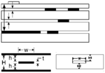
If in a region on the PCB board, over several layers we intentionally remove copper so that there is only dielectric FR4 in the area, then how should we calculate the thickness of this FR4 region?

First, if there is no copper, would FR4 layer over and immediately beneath the area expand to fill the area? I guess it is a must, because eventually board undergoes pressing, and evidently it is impossible for the FR4 layer above and beneath the empty copper region to touch each other. However, in this situation the density of the FR4 would also somehow changed, so would there be a significant change to its dielectric constant?
Second, when we are trying to calculate the thickness of the dielectric layer in this situation, should we calculate the copper thickness, even if it left empty and have been filled by expanded FR4? A problem which seems somehow related to this question is the calculation of “stripline” impedance, for which the thin copper is sandwiched by dielectric layers. I have checked several sources, some (as shown in the lower left) does include copper thickness in their formula, and some (as shown in the lower right) don’t.
Could someone help with this question?
Jacky
If in a region on the PCB board, over several layers we intentionally remove copper so that there is only dielectric FR4 in the area, then how should we calculate the thickness of this FR4 region?

First, if there is no copper, would FR4 layer over and immediately beneath the area expand to fill the area? I guess it is a must, because eventually board undergoes pressing, and evidently it is impossible for the FR4 layer above and beneath the empty copper region to touch each other. However, in this situation the density of the FR4 would also somehow changed, so would there be a significant change to its dielectric constant?
Second, when we are trying to calculate the thickness of the dielectric layer in this situation, should we calculate the copper thickness, even if it left empty and have been filled by expanded FR4? A problem which seems somehow related to this question is the calculation of “stripline” impedance, for which the thin copper is sandwiched by dielectric layers. I have checked several sources, some (as shown in the lower left) does include copper thickness in their formula, and some (as shown in the lower right) don’t.
Could someone help with this question?
Jacky