Continue to Site

Welcome to EDAboard.com

Welcome to our site! EDAboard.com is an international Electronics Discussion Forum focused on EDA software, circuits, schematics, books, theory, papers, asic, pld, 8051, DSP, Network, RF, Analog Design, PCB, Service Manuals... and a whole lot more! To participate you need to register. Registration is free. Click here to register now.

Did i get malfunctioning MCP3421

Status
Not open for further replies.

yefj

Advanced Member level 4
Joined
Sep 12, 2019
Messages
1,180
Helped
1
Reputation
2
Reaction score
3
Trophy points
38
Activity points
7,110
Hello,as shown In the datasheet bellow I have recreated the Data diagram using the 0XD0 address,
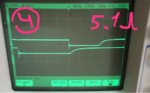
And instead of getting ACK after adress byte it gives me NACK,as shown in the scope photos bellow.
Did i ordered a malfunctioning MCP3421?
If there nothing to do ,i would like a suggestion for an ADC and thermal sensor (The LM35 i bought also didnt work)brands i could use on my breadboard.
Thanks.


1609407767240.png

1609407800548.png

1609408103334.png


1609408528405.png

1609408561645.png

1609408651944.png
 

Hello Barry,SDA is going LOW while SCL is high, i marked in red arrow the start section,then we have 9 clocks
0XD0 (8 bytes of adress and write) and the unfortunate NACK byte when SDA high on the 9th clock, and then we get a stop bit.and thats how it goes in a cycle over and over.
So i cant understand what do you mean my timing is wrong?

1609429711719.png
 

Your timing looks a little funny. Not sure, but I think Maybe SCL needs to go low while SDA is low (start). That’s the way ive always done it. Look at the data sheet diagram.
 

Start is LOW SDA While SCL is high,i have prior expirience with SI7021 sensor to confirm that.
 

The first falling edge of SCK looks worryingly close to the first rising edge of SDA. Are you sure a start condition is being sent?
A logic analyzer is more useful than a 'scope for this kind of issue.


Brian.
 
  • Like
Reactions: yefj

    yefj

    Points: 2
    Helpful Answer Positive Rating
Hi,

A useful scope picture fir this would be to show the first falling clock edge and the data in detail. Just zoom in.
We just need to see the "falling clock" to "data change" timing.

Klaus
 
  • Like
Reactions: yefj

    yefj

    Points: 2
    Helpful Answer Positive Rating
Hello Klauss,Will be done as soon as possible.
Thanks.
 

Hello Klauss, The photo bellow is for the same system using another scope.i used 5.1Kohms pullup registers for SDA and SCL.
The code i used is the same as i used for the EFR32fg14 on board SI7021 sensor.
the only difference now i that the forst byte is 0xD0 an we I use external I2C device MCP3421 device on the breadboard.
Start condition as i understand is just Lowering SDA whle SCL is high.
Is my device malfunctioning?


1609499179562.png
 

Hi,
We just need to see the "falling clock" to "data change" timing.
Impossible to get the timing information from your scope picture.

Zoom in on the first falling clock edge. Show the timing scale of the scope.

Klaus
 

Hello Klauss,The photo you requested shown bellow ,horisontal scale is 2us per DIV and the vertical is 2V per DIV.
I know that this scope is not as good as i presented in the first post,i cant present a more accurate photo in a few days if this zoomed waveform not detailed enough.

update:
Yes i see that its far from being detailed.
I will post a new photo as fast as possible.
Thanks.

1609500639319.png
 
Last edited:
Better - what concerns me is the stop condition is created by SDA going high while SCL is high. It wasn't possible to see if that was happening when the edges were so close. I still think it may be the cause of your problem. Apart from start and stop conditions, SDA changes should only occur when SCL has had time to be recognized as low by the slave device.

Brian.
 

  • Like
Reactions: yefj

    yefj

    Points: 2
    Helpful Answer Positive Rating
Hello 00Kam, How do i check for the true A2A1A0, in the data sheet shown bellow they say that its 000.
So 1101+000+0 (device+address+write)=0xD0.
Also they say that it needs those ressistors,they are not connected. i see that it also needs a capacitor.
I will connect and try it again on a more accurate scope.

UPDATE:Yes i think you are correct. the MCP3421 is only one chip on the device it has two capacitors and ressistors,
So there is no need to add anything.The only question which remains is reagrding the A2A1A0 adress.


1609579304234.png
1609578812081.png


1609579213936.png
 
Last edited:

there are three notes on this I2C MPC3421 i have concluded from the data sheet .
1- the on -board MCP3421 comes with two pull up 5kohm or "4.7komh" in operation frequency (100kH-400KH) so there is no need for connection external resistors as in the post #1.
2- also from data sheet check the true" Address option" (PRODUCT IDENTIFICATION SYSTEM )(A0-A2) by the type in your MCP3421 XX

part NO. XX X X /XX

Device Address option tape and reel

PRODUCT IDENTIFICATION SYSTEM
Address Options: XX A2 A1 A0
A0 * = 0 0 0
A1 = 0 0 1
A2 = 0 1 0
A3 = 0 1 1
A4 = 1 0 0
A5 = 1 0 1
A6 = 1 1 0
A7 = 1 1 1
as i see the code after the 0XD0 device address is "000" in scope. post#1.

3- from data sheet the MCP4321
The device communicates with Master
(microcontroller) through a serial I2C (Inter-Integrated
Circuit) interface and support standard (100 kbits/sec),
fast (400 kbits/sec) and high-speed (3.4 Mbits/sec)modes.
and "Barry" up loaded perfect link for I2C protocol i concluded that you have some thing up normal with
serial clock "SCL" when start bit goes from high-low "falling edge " for a hold time then SCL goes from H-L
"falling edge till the end of start bit . comparing with scope. post#1. the matter is different .


kamal
 
  • Like
Reactions: yefj

    yefj

    Points: 2
    Helpful Answer Positive Rating
Hi,

Please show your code. Give all informations, what libraries you use ... and so on.

Klaus
 
  • Like
Reactions: yefj

    yefj

    Points: 2
    Helpful Answer Positive Rating
hello
Regarding the "Address Options " focus in your board the part NO .of MCP4321XX (XX)means the address opition of your MCP4321 you are using .and in data sheet section 8
"PACKAGING INFORMATION" if your MCP4321 A0 on-board that is mean the address option A0 is (000) as you are doing but if your MCP4321A1 --->A1 the address option A1(001) and so on if you find that your MCP on-board differs . for example if you find the MCP in your board of address option with MCP4321A2--->A2 (010) the sending data is (fall address +writ )will be (1101 010 0) but not (1101 000 0).

kamal
 

Looking back at post #1, bottom photograph. Are you sure the resistors are 5.1K ? One looks correct, the other looks more like 1K.

There are already 4.7K pull-up resistors on the PCB anyway.

Brian.
 
  • Like
Reactions: yefj

    yefj

    Points: 2
    Helpful Answer Positive Rating
Hello,In order not overwelm with photos,i will present bellow two cases.One withought pullups resistors,and the other i
put 5.1Kohms resistor.
The full code is attached bellow.
In EFR32FG14 on the same PC10 PC11 we have the I2C external header and the SI7021 so i PUT PD15 to be 0 in order to disable SI7021 .
As you can see bellow withought any pullups on the PCB the SCL have very curved shape.
When i add 5.1Kohm it gets much better. shape but still the SDA RISES just as the SCL FALLS.
In both cases its like that.The full code is attached bellow.
In both cases i have periodic sturcture where i get NACK for the address.
What could cause such a thing? is it the device itself?

Thanks.

1609747516962.png

1609747608191.png

1609747668894.png


1609747941507.png

1609747989325.png
1609748129157.png

1609748245921.png

Code:
#include "em_usart.h"
#include "em_ldma.h"

/////////////////
#include "stddef.h"
#include "em_system.h"
#include "em_device.h"
#include "em_chip.h"
#include "em_cmu.h"
#include "em_emu.h"
#include "em_gpio.h"
#include "i2cspm.h"
#include "si7013.h"
#include "sl_sleeptimer.h"
#include "graphics.h"
#include "em_adc.h"
#include "bspconfig.h"


uint8_t com1[1] = {0x1C}; //config command

//page 20 of data sheet
uint8_t i2c_rxBuffer[4]; //[0]-2nd Byte [1]-3rd byte [2]-4th byte [3]-5th config byte
void initUSART1 (void)
{
    CMU_ClockEnable(cmuClock_GPIO, true);
    CMU_ClockEnable(cmuClock_USART1, true);

    // Configure GPIO mode
    GPIO_PinModeSet(gpioPortC, 8, gpioModePushPull, 0); // US1_CLK is push pull
    GPIO_PinModeSet(gpioPortC, 9, gpioModePushPull, 1); // US1_CS is push pull
    GPIO_PinModeSet(gpioPortC, 6, gpioModePushPull, 1); // US1_TX (MOSI) is push pull
    GPIO_PinModeSet(gpioPortC, 7, gpioModeInput, 1);    // US1_RX (MISO) is input
    GPIO_PinModeSet(gpioPortF, 7, gpioModeInput, 1);    // delay gpio

    // Start with default config, then modify as necessary
    USART_InitSync_TypeDef config = USART_INITSYNC_DEFAULT;
    config.master       = true;            // master mode
    config.baudrate     = 1000000;         // CLK freq is 1 MHz
    config.autoCsEnable = true;            // CS pin controlled by hardware, not firmware
    config.clockMode    = usartClockMode0; // clock idle low, sample on rising/first edge
    config.autoCsEnable = true;            // CS pin controlled by  firmware
    config.msbf         = true;            // send MSB first
    config.enable       = usartDisable;    // Make sure to keep USART disabled until it's all set up
    USART_InitSync(USART1, &config);

    // Set USART pin locations
    USART1->ROUTELOC0 = (USART_ROUTELOC0_CLKLOC_LOC11) | // US1_CLK       on location 11 = PC8 per datasheet section 6.4 = EXP Header pin 8
                        (USART_ROUTELOC0_CSLOC_LOC11)  | // US1_CS        on location 11 = PC9 per datasheet section 6.4 = EXP Header pin 10
                        (USART_ROUTELOC0_TXLOC_LOC11)  | // US1_TX (MOSI) on location 11 = PC6 per datasheet section 6.4 = EXP Header pin 4
                        (USART_ROUTELOC0_RXLOC_LOC11);   // US1_RX (MISO) on location 11 = PC7 per datasheet section 6.4 = EXP Header pin 6

    // Enable USART pins
    USART1->ROUTEPEN = USART_ROUTEPEN_CLKPEN | USART_ROUTEPEN_CSPEN | USART_ROUTEPEN_TXPEN | USART_ROUTEPEN_RXPEN;


    // Enable USART1
    USART_Enable(USART1, usartEnable);
    ////////////////////////////////////////////
    //UART INITLIZATION

    USART_InitAsync_TypeDef init = USART_INITASYNC_DEFAULT;


     // Enable oscillator to GPIO and USART0 modules

     CMU_ClockEnable(cmuClock_USART0, true);

     // set pin modes for UART TX and RX pins
     GPIO_PinModeSet(gpioPortA, 1, gpioModeInput, 0);
     GPIO_PinModeSet(gpioPortA, 0, gpioModePushPull, 1);

     // Initialize USART asynchronous mode and route pins
     USART_InitAsync(USART0, &init);
     USART0->ROUTELOC0 = USART_ROUTELOC0_RXLOC_LOC0 | USART_ROUTELOC0_TXLOC_LOC0;
     USART0->ROUTEPEN |= USART_ROUTEPEN_TXPEN | USART_ROUTEPEN_RXPEN;

}//end usart init

int main(void)

{

I2C_TransferSeq_TypeDef i2cTransfer;

I2C_TransferReturn_TypeDef result;


 I2CSPM_Init_TypeDef i2cInit = I2CSPM_INIT_DEFAULT;


 /* Chip errata */

 CHIP_Init();
 initUSART1();


 // Enabling clock to the I2C, GPIO, LE

 CMU_ClockEnable(cmuClock_I2C0, true);

 CMU_ClockEnable(cmuClock_GPIO, true);

 CMU_ClockEnable(cmuClock_HFLE, true);


 // Starting LFXO and waiting until it is stable

 CMU_OscillatorEnable(cmuOsc_LFXO, true, true);


 I2CSPM_Init(&i2cInit);

 // In order to enable the I2C0_SCL function in PC10 you need to use ROUTE 14

 // In order to enable the I2C0_SDA function in PC11 you need to use ROUTE 16

 //Also note that there's a GPIO pin PD15 that need to be set to high in order to route the signals to the sensor,

 // Using PC10 (SCL) and PC11 (SDA)

  GPIO_PinModeSet(gpioPortC, 10, gpioModeWiredAndPullUp, 1);

  GPIO_PinModeSet(gpioPortC, 11, gpioModeWiredAndPullUp, 1);


// GPIO_PinModeSet(gpioPortC, 10, gpioModeWiredAnd, 1);

//  GPIO_PinModeSet(gpioPortC, 11, gpioModeWiredAnd, 1);

  //Si7021 switch off

  GPIO_PinModeSet(gpioPortD, 15, gpioModePushPull, 0);


  // Enable pins at location 15 as specified in datasheet

  I2C0->ROUTEPEN = I2C_ROUTEPEN_SDAPEN | I2C_ROUTEPEN_SCLPEN;

  I2C0->ROUTELOC0 = (I2C0->ROUTELOC0 & (~_I2C_ROUTELOC0_SDALOC_MASK)) | I2C_ROUTELOC0_SDALOC_LOC16;

  I2C0->ROUTELOC0 = (I2C0->ROUTELOC0 & (~_I2C_ROUTELOC0_SCLLOC_MASK)) | I2C_ROUTELOC0_SCLLOC_LOC14;

  i2cTransfer.flags=I2C_FLAG_WRITE_READ;

 // i2cTransfer.addr=0xD0;//address with write
  i2cTransfer.addr=0xD0;//address with write

  i2cTransfer.buf[0].data=&com1[0];  // Config byte

  i2cTransfer.buf[0].len=1;    //number bytes in config bytes


  i2cTransfer.buf[1].data=i2c_rxBuffer;

  i2cTransfer.buf[1].len=4;    //4 bytes =3 data and 1 config byte

while(1)

{

  result=I2C_TransferInit(I2C0,&i2cTransfer);


  // Sending data

   while (result == i2cTransferInProgress)

   {

    result = I2C_Transfer(I2C0);

   }

   //When sending data ends
   //SPI sending data
   USART_SpiTransfer(USART1,i2c_rxBuffer[0]);
   USART_SpiTransfer(USART1,i2c_rxBuffer[1]);
   USART_SpiTransfer(USART1,i2c_rxBuffer[2]);

   //send UART
   USART_Tx(USART0, '\n');
      USART_Tx(USART0, i2c_rxBuffer[0]);
      USART_Tx(USART0, i2c_rxBuffer[1]);
      USART_Tx(USART0, i2c_rxBuffer[2]);
      USART_Tx(USART0, 'a');
      USART_Tx(USART0, '\n');


}


 }
 

Attachments

  • 1609748070802.png
    1609748070802.png
    1.2 MB · Views: 130

To repeat, yet again:

1) Your rise time still looks too long.
2) people keep telling you that you probably shouldn’t having SDA and SCLK transitioning simultaneously; you haven’t addressed that.
 

Hello Barry, I have addressed this issue :) the quate bellow.
I dont know why its like that with and without the pullup ressistors .i wish i knew what could be done to change this situation.even when i put by mistake 5.1Kohm and 1Khm at the first post still its the same phenomena.

What do you recommend to do?
Thanks.
" still the SDA RISES just as the SCL FALLS."
 
Last edited:

Status
Not open for further replies.

Part and Inventory Search

Welcome to EDABoard.com

Sponsor

Back
Top