Continue to Site

Welcome to EDAboard.com

Welcome to our site! EDAboard.com is an international Electronics Discussion Forum focused on EDA software, circuits, schematics, books, theory, papers, asic, pld, 8051, DSP, Network, RF, Analog Design, PCB, Service Manuals... and a whole lot more! To participate you need to register. Registration is free. Click here to register now.

Development board with FPGA GW1N-LV9LQ144C6/I5

FlyingDutch

Advanced Member level 1
Joined
Dec 16, 2017
Messages
457
Helped
45
Reputation
92
Reaction score
55
Trophy points
28
Location
Bydgoszcz - Poland
Activity points
4,954
Hello forum,

I designed a simple development board with FPGA from GowinSemi - IC model: GW1N-LV9LQ144C6/I5. Here is link to mouser.com with this product:

https://www.mouser.com/ProductDetai...W1N-LV9LQ144C6-I5?qs=wnTfsH77Xs6N/yGezJZrJQ==


Tis is basic FPGA with 8640 LUT and 120 I/Os in LQFP-144 case. The amount of resources allow conduct experiments with Soft-CPU (for example with RISC-V soft-cores). My main goal was to design FPGA development which is cheap, but is suitable for beginners. Apart the FPGA itself the board is equipped with:
1) 24 MHz clock circuit
2) LDO voltage controllers and switches for configuring FPGA I/O Banks (three voltages: 3.3V , 2.5V and 1.2 V
3) FPGA Mode switches (for boot mode)
4) Setup circuitry (Reconfig, Done etc.)
5) FPGA reset circuit
6) USB to JTAG based on FTDI chip FT 2232HL (allowing programing by USB socket)
7) JTAG Header for alternating programming by "Gowin Cable" external programmer
8) Additional 32Mb SPI flash IC
9) 8MB of PSRAM (Pseudo RAM) alowing big frame-buffers
10) DSub15 VGA connector
11) 8 user LEDs
12) 8 DIP-Switches
13) 5 Push Buttons
14) TF (uSD) card module
15) Simple audio output
16) 59 I/O pins led out to the three goldpin connectors

I wanted the FPGA kit had the opportunity to program by USB socket and did not require expensive external programer (Gowin "USB Cable"), hence the use of the FTDI chip . I also wanted the FPGA board bring out a large number of I/O pins. I don't plan to output differential pins (LVDS) with impedance and length control on PCB. Here is finished schematic:
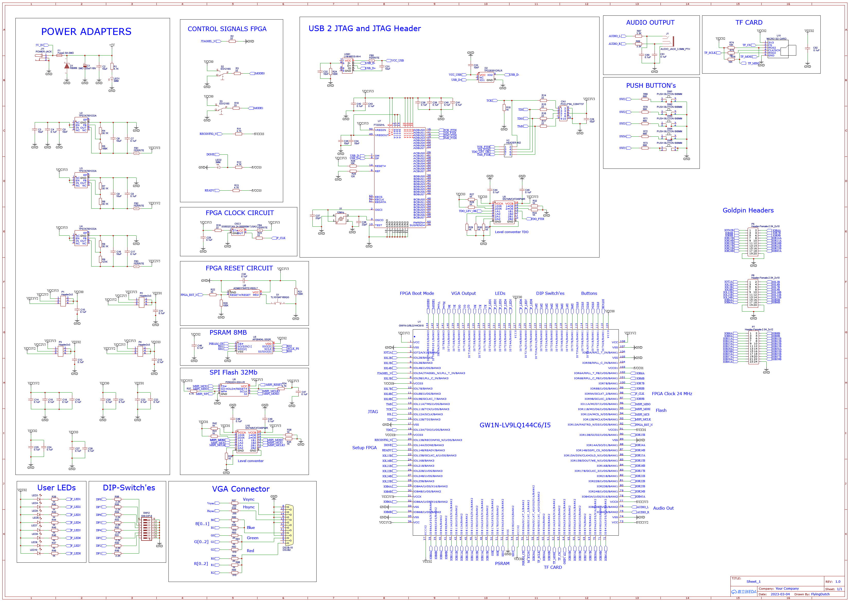
Schematic_Gowin_GW!N_LV9_LQ144_DevBoard_2023-05-02.png


It remains to design the PCB.
This is how the initial arrangement of components on the PCB looks like:
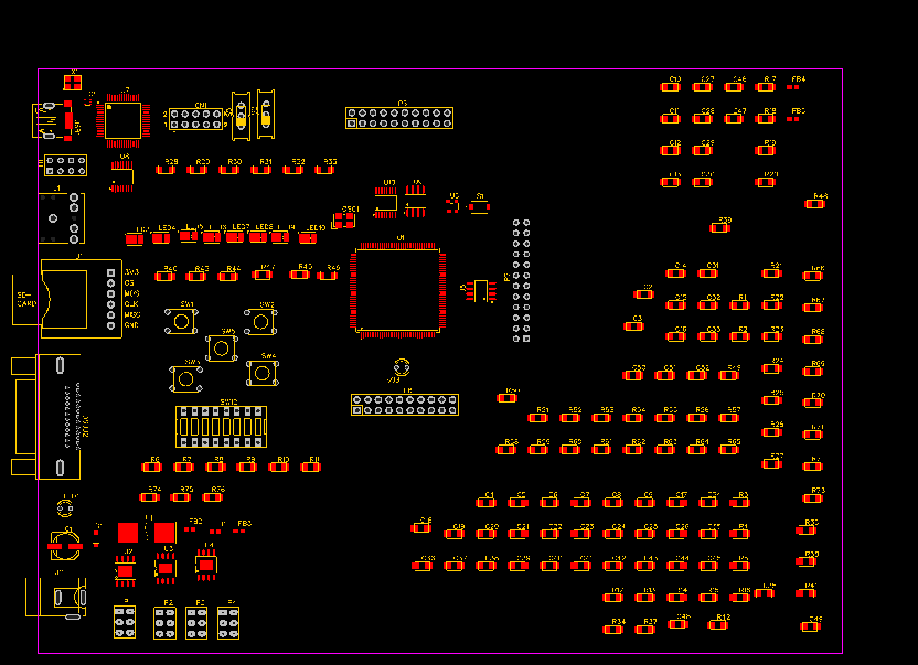
PCB_PCB_Gowin_GW!N_LV9_LQ144_DevBoard_02_2023-05-02.png


I will update the thread as I design the PCB.

Regards
 

Attachments

  • Schematic_Gowin_GW!N_LV9_LQ144_DevBoard_2023-05-02-1.pdf
    454.5 KB · Views: 104
As I know, members start a post here looking for questions, suggestions, etc, and the thread ideally remains open for replies until is is marked 'Solved'.
But I do not understand the intention of your thread.

I am of the opinion that your post is more of a blog or promotion work type. EDA-Board has a separate Blog section which is more suited for such work.

Please do not get the wrong opinion that I am against your post.
Hello,

@dpaul, I didn't write this post for promotion. I just design the cheap FPGA board I want to use and I thought that others might be also interested in it. I would like to know others' opinions about this board, also critical. I am not advertising Gowin FPGAs, but I am using them because they are cheap and still are available. I actually like Gowin FPGAs and their software and free IP Cores.
If it is not a proper place for this thread please move it to proper location :)

Thanks in advance
 
Hi,

My feedback:
On the PCB I see a lot of capacitors and/or resistors on the right side.
I can't find out their purpose.
But usually on FPGAs with high speed signals one wants the traces to be as short as possible.
So - for my taste - they are too far away from the FPGA.

Mind:
* the trace length causes impedance that can not be compensated by trace width/thickness
* it's not the true frequency (which depends on application) that causes EMI, but it's the signal rise/fall rate (for sure becomes multiplied by the frequency). Thus a long trace with just 1MHz may spread a lot of noise way above 1MHz. (And also pick up.. WiFi, cell phones, Bluetoooth...)
* a rock solid GND plane is a must.

Klaus
Hello @KlausST,

I just didn't finish the arrangement of the parts - they will be close to using it circuits. The placement of components will be optimized by me during the design phase of the PCB. I know the rules for high-speed signals (impedance and length control), but in the case of this board, only USB signals will be designed with impedance and length control (USB socket of FTDI chip). There are several differential signals pins on this FPGA chip (LVDS), but I am not willing to lead them out to goldpin headers using impedance matching (this board is for beginners for basic learning) and I assume that there will not be a need of using high-speed signals.
I am going to design a more advanced FPGA board based on the Gowin GW1N LV9 chip in the BGA256 case. On this second board, I will lead out LVDS signals and design traces on PCB with impedance and length matching. I am also planning to lead out HDMI output and DDR3 memory (which both are high-speed signals).
BTW: there will be a solid ground layer on PCB

Thanks for your comment and regards
 
@FlyingDutch
Again I am not questioning your motivation or intention.......just wanted to point out the place of posting.

btw - Now a days I see a lot of people promoting their work on LinkedIn. So other that creating blogs at various forums, I would suggest posting there too for better reach. If your network is with the relevant people there, then your contacts will read your posts and may comment on them.
 
Hello,

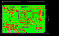
I has just finished the PCB board for this FPGA board. the PCB board has 6 layers and 141mm x 95 mm size.
Here are current schematics and PCB board:

PCB_PCB_Gowin_GW!N_LV9_LQ144_DevBoard_33_FinalRaw_2023-05-31.png


I also attache a Gerber file. I am going to post this project as open-hardware on my Github account. I am also planning to make operating manual for this board and various tutorials related to soft-CPU implementation.

Regards
 

Attachments

  • Schematic_Gowin_GW!N_LV9_LQ144_DevBoard.pdf
    449.4 KB · Views: 83
  • PCB_Gowin_GW!N_LV9_LQ144_DevBoard_33_FinalRaw_2023-05-31-2.pdf
    763.6 KB · Views: 81
  • Gerber_PCB_Gowin_GW!N_LV9_LQ144_DevBoard_33_FinalRaw.zip
    109.6 KB · Views: 81
No ground plane?
I thought the same.
Designing the green layer as GND plane should be less work than routing all the traces.
But I guess autorouter did the routing. Still don´t understand. So writing post#5 was a waste of time :-(

Klaus
 
No ground plane?
Hi,

in "Easy EDA" CAD and in JLPCB company there is not "blind vias" available so I can't make full layer (cooper area) a ground plane.

I thought the same.
Designing the green layer as GND plane should be less work than routing all the traces.
But I guess autorouter did the routing. Still don´t understand. So writing post#5 was a waste of time :-(

Klaus
Hi,
no @KlausST- this board hasn't been designed with autorouter - you are not right. Neither "EasyEDA" CAD nor JLCPCB company where I am going to make the PCB board doesn't support "blind vias" (vias beetwen two layers) - vias in this CAD connects all layers (so with solid ground plane I will have short circuits with many signals).This is the reason I cant fill cooper all over green layer. This board had been designed "by hand" - autoruter is not able to design such complex board. About your comment related to "high spedd signals" only USB signal is "high speed" on this board (and traces are designed with impedance and length matching).

Regards
 
in "Easy EDA" CAD and in JLPCB company there is not "blind vias" available so I can't make full layer (cooper area) a ground plane.
A ground plane with holes for vias between other layers is much better than no ground plane.
 
Hello,

as suggested I poured out all "ground" (green colur) layer with cooper. Earlier I had bad value of one parameter during pouring cooper. I am attaching altered version of PCB and gerber files.

PCB_PCB_Gowin_GW!N_LV9_LQ144_DevBoard_33_FinalRaw_2023-06-01.png
 

Attachments

  • PCB_PCB_Gowin_GW!N_LV9_LQ144_DevBoard_33_FinalRaw_2023-06-01.pdf
    1.1 MB · Views: 79
  • Gerber_PCB_Gowin_GW!N_LV9_LQ144_DevBoard02.zip
    216.4 KB · Views: 66
Hi,
in "Easy EDA" CAD and in JLPCB company there is not "blind vias" available so I can't make full layer (cooper area) a ground plane.
All my PCB layouts inlude a solid GND plane. Almost no PCB use blind vias.

Additional comments regarding layout:
* are you sure you want the vias in the SMD pads? In most cases you simply could avoid them.
* your power traces are rather small. May work for low currents... but for higher currents
* audio signals without DC blocking capacitor?
* why 680R in series with the push buttons? (I´d rather expect pull up)
* why 2k2 in series with the DIP switches? (I´d rather expect pull up)
* why 33R in series with the MODE switches?
* What´s R21 good for?
* Are you sure you don´t want OSC1 supply bypassed with a capacitor?
* Are you sure you want the LED current below 1mA?

Klaus

Added:
Usually one wants some mm gap between PCB outline and copper.
 
Last edited:
Hi,

All my PCB layouts inlude a solid GND plane. Almost no PCB use blind vias.

Additional comments regarding layout:
* are you sure you want the vias in the SMD pads? In most cases you simply could avoid them.
* your power traces are rather small. May work for low currents... but for higher currents
* audio signals without DC blocking capacitor?
* why 680R in series with the push buttons? (I´d rather expect pull up)
* why 2k2 in series with the DIP switches? (I´d rather expect pull up)
* why 33R in series with the MODE switches?
* What´s R21 good for?
* Are you sure you don´t want OSC1 supply bypassed with a capacitor?
* Are you sure you want the LED current below 1mA?

Klaus

Added:
Usually one wants some mm gap between PCB outline and copper.
Hi @KlausST ,

the DIP-switches and push buttons are based on "Mimas v.2" FPGA board (by Numato LAbs). I am using this board from several years and it works fine - see schematics:

https://numato.com/help/wp-content/uploads/2016/08/MimasV2Sch.pdf

https://numato.com/product/mimas-v2-spartan-6-fpga-development-board-with-ddr-sdram/

Both of them are used with internall pull-up from FPGA I/Os


why 33R in series with the MODE switches?

This is taken from Gowin reference board for FPGA series GW1N. ALso R21 is taken from reference board (Gowin).

Are you sure you want the LED current below 1mA?
these LEDs has 2mA nominal current.

Best Regards
 
Hi,

I see that the series resistors are used in the other designs. But still I see no reason for them. Three different values - without making sense.
They provide no filtering, no useful current limiting, no protection ... I call them useless.
On the same time they won´t harm - in so far I fully understand that your board works for yeras ...

Klaus
 

LaTeX Commands Quick-Menu:

Similar threads

Part and Inventory Search

Welcome to EDABoard.com

Sponsor

Back
Top