Continue to Site

Welcome to EDAboard.com

Welcome to our site! EDAboard.com is an international Electronics Discussion Forum focused on EDA software, circuits, schematics, books, theory, papers, asic, pld, 8051, DSP, Network, RF, Analog Design, PCB, Service Manuals... and a whole lot more! To participate you need to register. Registration is free. Click here to register now.

Determining Polarity

Status
Not open for further replies.

Mustaine

Member level 1
Joined
Mar 27, 2021
Messages
32
Helped
0
Reputation
0
Reaction score
0
Trophy points
6
Activity points
214
Hello friends
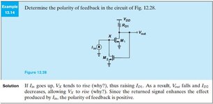
In the example on the fundamentals of microelectronics by razavi, there is a examples that i do not understand,
the example says if Iin increases Vx tends to rise but why is that? it is mosfet there is no gate resistance.
Also example says when Id2 falls it allows the Vx to rise i dont get it also
can you help me about that.
thanks in advance
 

Attachments

  • pics.JPG
    pics.JPG
    38 KB · Views: 114

Look at all devices connected to gate and current source. E = I x R, where else
is there a R that I can work against to create V ?


Regards, Dana.
 
Look at all devices connected to gate and current source. E = I x R, where else
is there a R that I can work against to create V ?


Regards, Dana.
so Vx rise because of the drain resistor of M2 right? i guess i can understand that but when it comes to current source i mean when Id2 decreases how Vx rise i can not understand that part, in my opinon Vx also decreases because of Id2 * (RoM2)
 

1618839821000.png


As Iin goes up, Vgs M1 goes up, Vds M1 goes down, Vgs M2 goes down, Rds M2 goes up, Vgs M1 goes up.....repeating


Regards, Dana.
 
Positive current Iin is required to establish negative loop gain over M1 and M2. Due to dominant pole at node Vx we expect a stable operating point rather than a "repeating" waveform.

I understand the doubts in post #1 so
that you are missing a load resistor for Iin and thus don't know how to calculate Vx. The circuit would even work with infinite load resistance due to the negative feedback topology, but in practice a current source has a finite output resistance of e.g. several Mohm.
 
The control loop is + fdbk. As Vgs rises on M1 its Vds drops allowing M2 Vds to rise which is
rising Vgs on M1, a + fdbk control loop.

Regards, Dana.
 
As Iin rises the voltage across the D-S goes up due to the finite on resistance - then you get the +ve feedback ...
 
thank you all of your replies friends i guess i get the point,
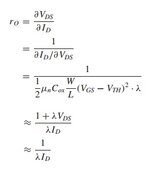
when we increase Iin Vx rises becaus of the ro of the M2,....,
Vout falls so that Vgs of M2 falls Id2 falls therefore according to the equation below(design of analog cmos ic by behzad razavi) ro2 rises and Vx rises (Iin*ro2).
i hope the inferences i make, makes sense.
 

Attachments

  • razavi.jpg
    razavi.jpg
    11.5 KB · Views: 95

Status
Not open for further replies.

Part and Inventory Search

Welcome to EDABoard.com

Sponsor

Back
Top