Welcome to our site! EDAboard.com is an international Electronics Discussion Forum focused on EDA software, circuits, schematics, books, theory, papers, asic, pld, 8051, DSP, Network, RF, Analog Design, PCB, Service Manuals... and a whole lot more! To participate you need to register. Registration is free. Click here to register now.
Behind the basics there are some nuances that relate to
things like suppressing / minimizing RTS (RTN) noise, field
control and so on. Applications which need very low dark
current and cryo operation care a lot about this; a receiver
for short haul fiber optics, less so.
Give some thought to your application care-abouts, and
the literature may help you with the finer points of device
construction.
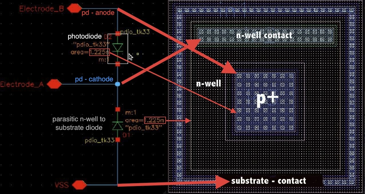
You just need one photodiode in layout: the other one (in schematic) is a parasitic diode between n-well and substrate. See this image: The area of the parasitic diode (the n-well area) is bigger than the pd (the p+) area.
The quadratic structure outside around the p+ diffusion area is the border between two recognition areas, s. this post.
Seems ok. If (and which) recognition layers are necessary for the LVS check to match, depends on your PDK's extract rules.
You wouldn't need the extra n-well contact, the n+ guard ring contacts are enough. So you could save some area: the n-well diffusion area can be with min. spacing outside the n+ guard ring, and the p+ substrate guard ring may have min. spacing to the n-well.
This site uses cookies to help personalise content, tailor your experience and to keep you logged in if you register.
By continuing to use this site, you are consenting to our use of cookies.