Continue to Site

Welcome to EDAboard.com

Welcome to our site! EDAboard.com is an international Electronics Discussion Forum focused on EDA software, circuits, schematics, books, theory, papers, asic, pld, 8051, DSP, Network, RF, Analog Design, PCB, Service Manuals... and a whole lot more! To participate you need to register. Registration is free. Click here to register now.

Designing a simple Common Emitter amplifier circuit.

Status
Not open for further replies.

Shayaan_Mustafa

Full Member level 5
Joined
Jan 16, 2011
Messages
267
Helped
0
Reputation
0
Reaction score
0
Trophy points
1,296
Activity points
3,213
Hello experts!

I am newbie on this forum.
Someone told me that www.edaboard.com is the best forum of electronics.
I am a student of electronics engineering.

I have studied analog electronics. But don't have much command, how to design even a simple circuit i.e. how to predict the values of components like capacitors, resistors, etc.

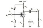
Here is my circuit below. For simplicity I am starting with CE amplifier configuration.

How to know that what value of resistors of capacitors to be used.

I have supplied 18VCC.

Thanks in advance.
 

Attachments

  • npnce3.jpg
    npnce3.jpg
    19.8 KB · Views: 102

welcom Shayaan_Mustafa :)

as I know you can't design amplifier without knowing some values like\[ R_E \]and\[ R_C\] and\[ \beta\] .

when you have sufficient elements to design you can start.

designing relations -which is true and used in design- are:
\[
I_{CQ}=\frac{V_{CC}}{R_{ac}+R_{dc}}
\]

\[
R_B=0.1 * \beta * R_E
\]

\[
R_1=\frac{R_B}{1-\frac{v_{BB}}{v_{CC}}}
\]
\[
R_2=\frac{R_B V_{CC}}{V_{BB}}
\]
at most time design is to find the value of\[ R_1\] and\[ R_2 \]which can select the type of work area and the Q-point which is the goal in ac and dc for prober using of amplifier .

i hope this help .

best regards .
 

Hello Shayaan_Mustafa,

I think - before starting to calculate some values based on given formulas - as the first step you should try to understand the meaning and the task of each part of the circuit.
What is the task of Re and why is there a capacitor Ce? Only then you really can understand the content of the formulas - and the region in which you can/must select the values.


Thanks for reply. And I have already review that site.
If I would have design that circuit with the help of data that is given on that site. Then I never register to this site.
I will lose the chance to gain some knowledge about designing circuits.

---------- Post added at 16:30 ---------- Previous post was at 16:12 ----------

welcom Shayaan_Mustafa :)

as I know you can't design amplifier without knowing some values like\[ R_E \]and\[ R_C\] and\[ \beta\] .

when you have sufficient elements to design you can start.

designing relations -which is true and used in design- are:
\[
I_{CQ}=\frac{V_{CC}}{R_{ac}+R_{dc}}
\]

\[
R_B=0.1 * \beta * R_E
\]

\[
R_1=\frac{R_B}{1-\frac{v_{BB}}{v_{CC}}}
\]
\[
R_2=\frac{R_B V_{CC}}{V_{BB}}
\]
at most time design is to find the value of\[ R_1\] and\[ R_2 \]which can select the type of work area and the Q-point which is the goal in ac and dc for prober using of amplifier .

i hope this help .

best regards .

Thanks for reply

What is Rac and Rdc?

We can calculate RE from
RE=\[\frac{VRE }{IE }\]

We can also calculate β from
β=\[\frac{IC }{IB }\]

---------- Post added at 16:33 ---------- Previous post was at 16:30 ----------

Hello Shayaan_Mustafa,

I think - before starting to calculate some values based on given formulas - as the first step you should try to understand the meaning and the task of each part of the circuit.
What is the task of Re and why is there a capacitor Ce? Only then you really can understand the content of the formulas - and the region in which you can/must select the values.

Thanks for reply

RE is to easily ground signals.
CE is a bypass capacitors which ground AC signals of high frequency.

Am I right?

I just want to gain complete command on analog electronics.
 

RE is to easily ground signals.

What means "easily"? Wouldn't it be easier without any resistor? Did you hear already about feedback?

CE is a bypass capacitors which ground AC signals of high frequenc

Why? What is the goal to be achieved?
 

Thanks for reply

What is Rac and Rdc?

We can calculate RE from
RE=\[\frac{VRE }{IE }\]

We can also calculate β from
β=\[\frac{IC }{IB }\]

welcome :)

Rac and Rdc is the equivalent resistance in emitter-collector circuit in dc/ac . for example for common emitter configuration
\[R_{ac}=R_E + R_C || R_L . \]

\[R_{dc}=R_E + R_C .\]

if we consider that \[R_E\] is not bypassed by a capacitor and the load \[R_L\] is connected through capacitor .

capacitor is open circuit in dc because \[ X_C = \frac{1}{j2 \pi f c} \] and f=0(ideal) in dc and varies in ac .

and \[\beta\] can by known from the datasheet of amplifier .
 

RE is to easily ground signals.

What means "easily"? Wouldn't it be easier without any resistor? Did you hear already about feedback?

CE is a bypass capacitors which ground AC signals of high frequenc

Why? What is the goal to be achieved?

Thanks for reply.

Yes I have heard about feedback, +ve and -ve. And I also their concepts too.
But here RE is not as a feedback resistor. It is not to degenerate the signal here. I think so.

And I know CE here is a bypass capacitor which grounds signals of high frequencies.
If it is not here so signals will not be able to ground easily and create distortion at the output. Am I right?

---------- Post added at 20:02 ---------- Previous post was at 19:57 ----------

welcome :)

Rac and Rdc is the equivalent resistance in emitter-collector circuit in dc/ac . for example for common emitter configuration
\[R_{ac}=R_E + R_C || R_L . \]

\[R_{dc}=R_E + R_C .\]

if we consider that \[R_E\] is not bypassed by a capacitor and the load \[R_L\] is connected through capacitor .

capacitor is open circuit in dc because \[ X_C = \frac{1}{j2 \pi f c} \] and f=0(ideal) in dc and varies in ac .

and \[\beta\] can by known from the datasheet of amplifier .

Oh yes.
That is what I want to understand. This help me a lot. Now I try to solve my circuits with the given equation and assuming that I have load resistor RL=1.2k

If I have any problem or query about my circuit then I will refer to expert on www.edaboard.com

Thanks a lot.
 

Yes I have heard about feedback, +ve and -ve. And I also their concepts too.
But here RE is not as a feedback resistor. It is not to degenerate the signal here. I think so.

RE provides dc feedback (independent on CE) - thereby stabilizing the operating point.


And I know CE here is a bypass capacitor which grounds signals of high frequencies.
If it is not here so signals will not be able to ground easily and create distortion at the output. Am I right?

No, the opposite is true. Without CE you also will have signal feedback - thereby reducing distortions.
______________
Perhaps now you understand my recommendation regarding understanding the purpose and the effect of each part.

Regards
LvW
 

RE provides dc feedback (independent on CE) - thereby stabilizing the operating point.

No, the opposite is true. Without CE you also will have signal feedback - thereby reducing distortions.
______________
Perhaps now you understand my recommendation regarding understanding the purpose and the effect of each part.

OK. You mean if RE is not present here the I will get my output as DC shifted. Is it?

And if absence of CE reduces distortion at output(as you said in last post Without CE you also will have signal feedback - thereby reducing distortions.) then why we use CE as a bypass capacitor?

And one thing I know that at low VCC we don't need to use CE and RE like at 6VCC. Then why it is so. Give the reason of this in the light of your statement i.e. Without CE you also will have signal feedback - thereby reducing distortions.

Thanks.
 

OK. You mean if RE is not present here the I will get my output as DC shifted. Is it?

The normal approach is a redesign of all values in case of RE=0 (operating point needs to be recalculated).

And if absence of CE reduces distortion at output(as you said in last post Without CE you also will have signal feedback - thereby reducing distortions.) then why we use CE as a bypass capacitor?

Because everything in circuit design is a trade-off. Without CE you have more gain, but also more distortions.
In many cases, such a trade-off is implemented by dividing RE in two parts (and put CE only across one part).

And one thing I know that at low VCC we don't need to use CE and RE like at 6VCC. Then why it is so. Give the reason of this in the light of your statement i.e. Without CE you also will have signal feedback - thereby reducing distortions.

No, it's not true that you "don't need to use CE and RE". Perhaps somebody does not want a design with RE||CE - that's all. I's up to the user.
Remember my words: You have to understand the meaning, the task and the effect of each element. Only then you can decide if you want DC and/or AC feedback or not.
 

Correction (thanks to Mister-RF): "Without CE you have more gain" to be replaced by "With CE....".

---------- Post added at 09:53 ---------- Previous post was at 09:10 ----------

Only now I took the time to have look on the formulas as given by Y.T-comp
Mustafa, don't use this set of formulas. It is wrong! Y.T._comp does not realize that a BJT works as a current source.
 

Now I am little bit confusing here.
I want to understand some theory about common emitter.

Now I have some questions,
1)Why we use capacitor at the base of the circuit?(Answer: To decouple DC so that our signal that is reaching to base of the transistor is not to be DC shifted that's why it is called "Coupling capacitor". If it is not then we get our signal DC shifted from the ground level). And why we use capacitor at the emitter of the circuit i.e. CE?(Answer: Because we want signal to be ground easily. If capacitor is not placed there then we will have less gain.)

2)Why we use resistors at collector and at emitter?(Answer: So that we could get stability if it is not here then we get distortion at the ouput signal).

Are my three answers right?

Thanks
 

Mustafa, sorry but nothing is correct.
You really should try first to learn some BJT amplifier basics. There are a lot of sources (books, articles) that can be found in the internet.
 

Mustafa, sorry but nothing is correct.
You really should try first to learn some BJT amplifier basics. There are a lot of sources (books, articles) that can be found in the internet.

OK.
So I think I should start a new start in which I could learn some basics of this configuration of BJT i.e. common emitter.

Then I will post my new post of designing circuit.
And I hope all you people specially you LuW will help me. This forum is really so helpful.

Thanks for everyone specially you LuW.
 

OK, fine. That's a good idea.
Recommendation: Don't spend to much time for transistor physics and for the real function principle of Bipolars. Instead, realize that (and why) the transistor acts as a controlled current source and understand the role of each part (resistors, capacitors) in amplifier circuits. Have a look into data sheets and characteristic curves like Ic=f(Vbe) and Ic=f(Vce) for Ib=constant.
Good luck
 

Status
Not open for further replies.

Similar threads

Part and Inventory Search

Welcome to EDABoard.com

Sponsor

Back
Top