Continue to Site

Welcome to EDAboard.com

Welcome to our site! EDAboard.com is an international Electronics Discussion Forum focused on EDA software, circuits, schematics, books, theory, papers, asic, pld, 8051, DSP, Network, RF, Analog Design, PCB, Service Manuals... and a whole lot more! To participate you need to register. Registration is free. Click here to register now.

[SOLVED] Design the RF output path of wireless MCU (ATmega128RF)

Status
Not open for further replies.

alexxx

Advanced Member level 4
Joined
Apr 17, 2011
Messages
1,013
Helped
273
Reputation
552
Reaction score
270
Trophy points
1,383
Location
Greece
Activity points
7,936
Hi!

I use ATMEL ZigBit Modules the past 1.5 year, and now I think I will move on to ATmega128RF design (wireless MCU). It is my first touch with the RF analog part.
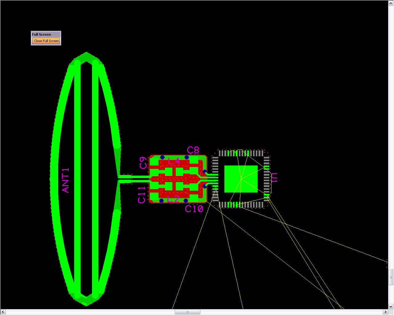
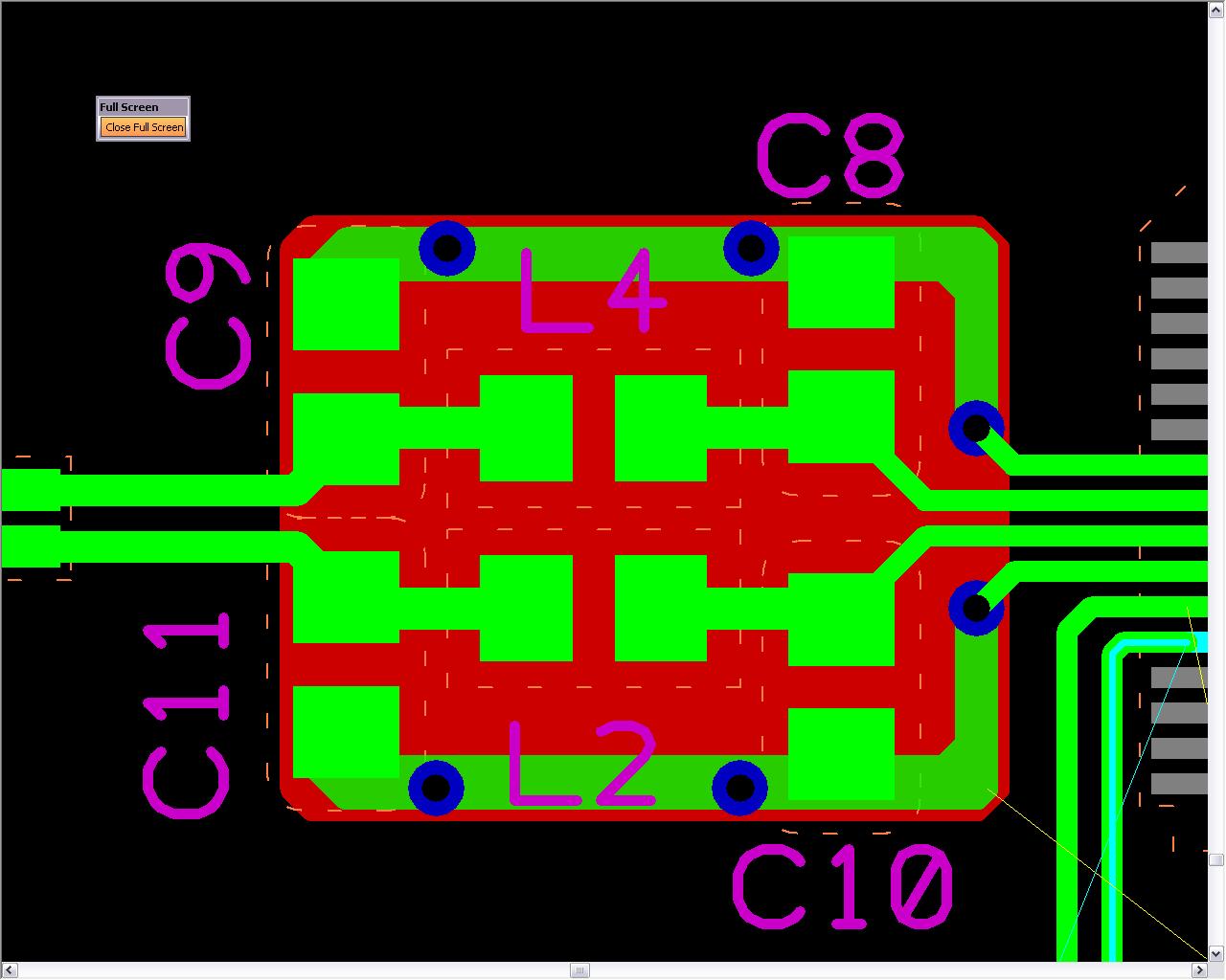
So about the RF part of the design. It is differential from the MCU (RFP, RFN), it will not include a BalUn and the antenna will be a pcb antenna. I use Atmel RZRaven Boards as reference. At page 14 of Hardware User's guide, in the RF output path, 6 passive components are involved, 4 capacitors and 2 inductors.
What is their use? What will happen if I don’t place them? What will happen if their values are not the same as the reference design?

Thanks in advance.
 

What will happen if I don’t place them?

This is a lowpass filter, to meet the regulations (out-of-band transmitted power).
Depending on the values, it can also be used for antenna impedance matching.
 

volker_muehlhaus said:
Depending on the values, it can also be used for antenna impedance matching.

Thank you volker_muehlhaus for your answer. So if it can be used for impedance matching, then I do not have to worry about trace length, width and height?
 

So if it can be used for impedance matching, then I do not have to worry about trace length, width and height?

For RF lines, you should think about line width/height. If that line impedance is chosen to match the source and load impedance, the line length can be chosen as needed.

In case of doubt, stay with the values given in the application note.
 

I will definitely stick to the AN values.
However if this circuit is used for impedance matching, then if impedance is matched, why do I have to worry about line dimensions?
Do you mean that impedance is matched, but I have to think dimensions to match it exactly to 50 Ohms?
 

However if this circuit is used for impedance matching, then if impedance is matched, why do I have to worry about line dimensions?

The line will transform the output impedance of the filter to another value, depending on the line parameters. In this case, the impedance transformation will depend on the line length also. See attachment.

But if we choose Zoutput = Zline = Zantenna, then we can choose the line length as needed, and there will be no additional impedance transformation.

Do you mean that impedance is matched, but I have to think dimensions to match it exactly to 50 Ohms?

Match everything to the same impedance. We usually want 50 Ohm, so that you can replace the antenna with a measurement instrument etc.
 

Attachments

  • transformation.JPG
    transformation.JPG
    62.3 KB · Views: 122

From what you told me until now volker_muehlhaus, I understood that:

1) From tranceiver's RFP and RFN outputs, the lines should be ideally like "twins" until they reach antenna, same length, width, curving etc, so that same impedance will be kept with each other.

2) If I use an inductance in series with the RF line, then inductor's ohmic resistance should be calculated in the total line impedance.

Are those two assumptions correct?

volker_muehlhaus said:
But if we choose Zoutput = Zline = Zantenna, then we can choose the line length as needed, and there will be no additional impedance transformation.

This is the critical point of the design.
If we assume that Zoutput = Zantenna = 50 Ohm, then how can I design a 50 Ohm line? I mean that I don't have a board in front of me to measure it with the Ohmeter, but I have to calculate it and then design it on my layout design software. How can I calculate the RF line impedance?

Thanks again.
 

1) From tranceiver's RFP and RFN outputs, the lines should be ideally like "twins" until they reach antenna, same length, width, curving etc, so that same impedance will be kept with each other.

Correct. Fortunately, it's not super critical at this frequency. If the lines are really short, then they are not critical. So it dependns on your layout.

2) If I use an inductance in series with the RF line, then inductor's ohmic resistance should be calculated in the total line impedance.

Ohmic losses of the filter are not part of the transmission line. If anything, I would include ohmic losses at the chip/transceiver side.

How can I calculate the RF line impedance?

I forgot that your lines are differential. Maybe the output impedance is 50+50 Ohm then.

One possible option is the free Sonnet Lite EM simulator, but that requires a little time to learn that tool.
Polar also have software to calculate impedance controlled transmission lines.

There are also some line calculators on the web, but I do not have the time now to document things for differential lines. If you go for that, just make sure that you look up the difference between differential impedance and odd mode line impedance.
 

I have done a great progress thanks to you volker_muehlhaus. A few more "dark spots" left.

I see RF SMD passive parts at 2.4GHz frequency, being 0603 size tops. I have 0805 parts at the store right now and I am thinking of using these parts.

1) Will 0805 size have negative effects on the RF part of the design, or is it OK to use them for now?

2) Is it better if those parts (independetly of their size) had round corners pads instead of 90 degrees angled? I heart it is better to have rounded pads.
 

alexx

to minimize risks in your application, let me suggest to you to post here both the Atmel PCB detailed layout and your layout, including vias, ground planes from IC pins to antenna.

The community can give you a feedback about the possible mistakes or optimization needed.

I hope it can help.

Mazz
 

1) Will 0805 size have negative effects on the RF part of the design, or is it OK to use them for now?

You can use them.

2) Is it better if those parts (independetly of their size) had round corners pads instead of 90 degrees angled? I heart it is better to have rounded pads.

Rectangular pads are fine. I see no technical reason to use rounded pads.
 

Thank you so much volker_muehlhaus for your assistance.

mazz said:
post here both the Atmel PCB detailed layout and your layout

I left the office for now, when I get back tomorrow I will do that, thank you too for your responce mazz.
 

Unfortunately ATMEL gives no recommended layout in the datasheet, just an application schematic.

My layout is below:


From MCU, through low pass filter, to antenna. Is the ground plane on bottom (red) layer OK?

Thank you.
 

Your Layout seems a good one, I will add some comments:

1. In their datasheet they declare to have 100+j0 differential impedance both in TX and in RX. This filter doesn't modify too much the impedance seen from the antenna when loaded with 50 Ohm (single ended), it means that is used only to filter out some TX harmonics.

2. It is under your responsability the specification for the differential antenna: to work properly it has to be 100+j0 differential.

3. Used L,C values of filter are small. In 0805 their SRF should be high enough to be safe for the filter response.

4. Embed the GND around the filter in a larger copper area and use many vias to GND around it. Extend also the bottom GND accordingly. Also connect the GND pins of the device direcly to exposed pad. Minimize the distance between the filter and the device, try to keep parasitic inductance of track in the 1-2 nH range.

5. If you need to keep antenna far from the filter, design the differential lines to have a differential impedance of 100 Ohm. You can use a small software (free) TXLINE (https://web.awrcorp.com/content/Downloads/TXLine.zip) to design them based on your PCB stack.

You're on the right way.

Mazz
 
Wow thank you Mazz, those are helpfull suggsetions!

So how much the filter's L, C values should be?

I will update my design and post it again, thank you!
 

Maybe I wasn't clear enough about L,C.

I mean that 1,2pF cap in 0805 has a self frequency resonance that is roughly 7GHz (you can check it in Murata web pages for example), that is far enough from 2.45GHz.
The same is true for the inductor.

Mazz
 

OK, so here is my design updated. More copper, more vias, and antenna got closer to the filter. The only thing I couldn't do is get the MCU closer to the filter, but there are others tracks that should leave from the MCU. And because of the GND pad under it, tracks cannot leave under the microcontroller and so I can't do much about it.


Status
Not open for further replies.

Part and Inventory Search

Welcome to EDABoard.com

Sponsor

Back
Top