Continue to Site

Welcome to EDAboard.com

Welcome to our site! EDAboard.com is an international Electronics Discussion Forum focused on EDA software, circuits, schematics, books, theory, papers, asic, pld, 8051, DSP, Network, RF, Analog Design, PCB, Service Manuals... and a whole lot more! To participate you need to register. Registration is free. Click here to register now.

Design of Low Drop-out Voltage Regulator

Status
Not open for further replies.

subbu2

Newbie level 6
Joined
Apr 3, 2014
Messages
12
Helped
0
Reputation
0
Reaction score
0
Trophy points
1
Activity points
101
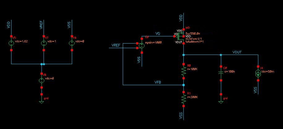
I am designing an LDO with following specs..
Vin : 1.8V +/- 10%
Vout : 1.5V +/- 3%
Vref : 1V +/- 1%
Iload : 0 to 50mA
Ext Cap : 100nF +/- 20%
PSR : >40dB upto 10MHz


please suggest me the way forward (where to begin the design wat parameters and architectures to look at etc.)..I have read abt the Single stage diff amp and abt miller compensation after adding second stage and yet to start wit the design.
 
Last edited:

Hi subbu2,

This spec is little bit interesting. Look at the Vin variation 1.8 +/-10% means that the minimum voltage will be 1.62V.
That means thee Power FET will have to provide 50mA current maintaining 1.5V at the output with only 120mV of VSD. Which again means that your Power FET will operate in linear region most of the time (specially when load is 50mA).

Start with the sizing of the Power FET first. Try to observe the Vsg voltage variation when load shifts from 0 to 50mV. This Vsg variation will give you the required swing at the output of the error amplifier. Then you can go ahead and choose your amplifier architecture.

Your load cap is big 100nF that means it will, most likely, be the dominant pole in the loop. Think when do we apply Miller Compensation? Will it work here?

One more thing you don't have a settling time spec. If you have one it will help you to target the loop Bandwidth and phase margin.

Hope this will help ... :)
 
Thank u Siddhartha Hazra sir for ur kind specific reply...I will now look into power mosfet details..if possible pls explain the d difference betn usual mosfet and power mosfet and how its used in LDO..
and how much gain is expected from the error amplr, do i need two stage amplifier..?
js thank u too i will c d datasheet u have given.. :)
 
Last edited:

Hi subbu2,

I will now look into power mosfet details..if possible pls explain the d difference betn usual mosfet and power mosfet and how its used in LDO..
and how much gain is expected from the error amplr, do i need two stage amplifier..?

Power FET is just a normal MOSFET with size big enough to supply 50mA current (in your case). As its is supplying power to the load that is why it is called Power PFET.

Do you have a reference voltage variation specification ..... If the reference will varies by +/-1.5% then your Output of the LDO will directly have +/-1.5% variation. So the remaining +/-1.5% (as the total spec is +/- 3%) will come from offset & dc gain of the loop. Set your architecture accordingly.

Two stage amplifier is generally avoided as the total loop will have three poles so it would be hard to compensate. So you may use cascode .... again it will have limited swing ah the output. As I mentioned i my earlier post that after sizing your Power FET you will get to know the Vgs variation as you load switches from 0 to 50mA. Check whether your cascode will support this change or not.

You will find lots of papers online .... go through them .... hope they will help ...
 
  • Like
Reactions: subbu2

    subbu2

    Points: 2
    Helpful Answer Positive Rating
Try to observe the Vsg voltage variation when load shifts from 0 to 50mV. This Vsg variation will give you the required swing at the output of the error amplifier. Then you can go ahead and choose your amplifier architecture.

Can u pls elaborate on tis..and how to do it on cadence..
 

Can u pls elaborate on tis..and how to do it on cadence..

Hope the picture attached will help. Keep sizing the Power FET till the desired Vg is obtained. This Vg will help in deciding output swing required at the error amp output.

The VCVS used acts as an error amplifier. The gain 1000 is just for test purpose. Actual gain requirement may vary.

 
Though i did not design the LDO for your specs..but the structure on CMOS may look something like shown in figures attached. I used folded cascode opamp for error amplifier with output stage W/L chosen for 10mA output current. My supply voltage varies from 3.2V to 4.2V.

 
  • Like
Reactions: subbu2

    subbu2

    Points: 2
    Helpful Answer Positive Rating
Thank u SIDDHARTHA HAZRA i will follow ur circuit and try to design power MOSFET...i wil ask u further clarifications once i do it:)

viperpaki007...can u please explain me the steps u followed to design this circuit from specs..
 

Hi subbu2

Are you interesting in design capacitorless LDO? I am designing it now. If you do I will give you paper about it
 
  • Like
Reactions: subbu2

    subbu2

    Points: 2
    Helpful Answer Positive Rating
Hi Subbu,

My design is essentially a two stage folded cascode rail-to-rail opamp with 2nd stage M13 transistor acting as pass transistor for the output current. Rst_ldo and Cst_ldo are there to make the system stable using miller compensation technique. Transistors MN0, M19,M15, M20 and M10 constitute bias circuit for opamp. MN10 and MN11 are main trans-conductance amplifiers for the folded cascode opamp. I designed the LDO for the following specs:

Vdd= 3.5-4.2V, Iload = 10mA, Vout =3.3V, Cl= 100f.

LDO, output stage transistor M13 W/L was chosen such that it can sustain 10mA current with small overdrive voltage. If you are unsure how to design a folded cascode opamp, you can take help from video lectures from this link or read Razavi CMOS.

https://www.satishkashyap.com/2012/02/iit-video-lectures-on-analog-integrated.html
 
  • Like
Reactions: subbu2

    subbu2

    Points: 2
    Helpful Answer Positive Rating
Hi subbu2

Are you interesting in design capacitorless LDO? I am designing it now. If you do I will give you paper about it

U can send me d link of d paper..bt presently i have to meet the specs which i have told abv, as a part of my project

- - - Updated - - -

Hi Subbu,

My design is essentially a two stage folded cascode rail-to-rail opamp with 2nd stage M13 transistor acting as pass transistor for the output current. Rst_ldo and Cst_ldo are there to make the system stable using miller compensation technique. Transistors MN0, M19,M15, M20 and M10 constitute bias circuit for opamp. MN10 and MN11 are main trans-conductance amplifiers for the folded cascode opamp. I designed the LDO for the following specs:

Vdd= 3.5-4.2V, Iload = 10mA, Vout =3.3V, Cl= 100f.

LDO, output stage transistor M13 W/L was chosen such that it can sustain 10mA current with small overdrive voltage. If you are unsure how to design a folded cascode opamp, you can take help from video lectures from this link or read Razavi CMOS.

https://www.satishkashyap.com/2012/02/iit-video-lectures-on-analog-integrated.html


thank u for explaining ur schematic...and yes i have been referring IIT video lectures (by nagendra krishnapura - d link u have mentioned) for past few months
 

Hi everyone
I am desinging capless LDO at vin = 1.8v vout = 1.6v . My maximum load current is 100mA and minimum 50uA. I got good phase margin (63 at 50uA and 86 at 100mA). The issue for me is the vout undershoot and overshoot when i switch loading current. I have picture loading for reference and hope anyone can help me with this. Thanks a lot


Hope the picture attached will help. Keep sizing the Power FET till the desired Vg is obtained. This Vg will help in deciding output swing required at the error amp output.

The VCVS used acts as an error amplifier. The gain 1000 is just for test purpose. Actual gain requirement may vary.


Sir I simulated the circuit u had suggested..I plotted Vg vs w for w varying from 1um to 20um but the Vg is in the range of 1.15V to 1.25V which means the power MOS is cutoff...and for case 2 I am getting some error in cadence.
these are the screen shots.

Screenshot-1.pngScreenshot-3.pngScreenshot-11.pngScreenshot-12.png
 

Hi,

See the size of the power FET will remain fixed whether you pull out 0mA or 50mA. As the Power FET has to support 50mA so you must size it for 50mA only (not for 0mA). At 50mA try to keep the Vg node lower so that the MOSFET is in saturation. When the current goes to 0mA then your Power FET gate voltage will automatically go high as its W/L is for high current. So at low load VSG requirement is low. You MOSFET may enter cut-off.

To avoid cutoff on thing you can go is to use smaller resistance (in Kohms). See there are two current paths to which the Power FET supplies current. One is the load which sometimes draws 50mA & sometimes 0mA and the Resistor devider that draws a fixed current = 1.5/(3R) ........

Now when your load is 0mA and you have 1M+2M resistor then total current through the Power FET = 0mA + 1.5/3M = 0mA + 500nA = 500nA only ..... that is why your FET is in cut-off. Try to burn around 5-10uA in the resistor divider (not more than that). And for practical reasons resistor of Mohms will take up huge layout area so generally not used.

If you are having convergence issues then do not give a DC sweep of the W. Just use W one at a time .... I see that 1uA is giving some problem .... Another thing you may try is not to use ideal current source instead use a resistor of R=1.5/50mA .... try to find a W at which the output rises to 1.5V as the resistors will not draw 50mA (as it is not a current source) unless you size the PFET to such a value that it will charge the cap to 1.5V.

If still the convergence issue exists ....the go through Spectre user manual ...there are few techniques ....
 
  • Like
Reactions: subbu2

    subbu2

    Points: 2
    Helpful Answer Positive Rating
I reduced the value of R1 and R2 to 100k and 200k so that they will draw 5uA of current if Vo is 1.5V ...instead of load current source of 50mA i have used 30 ohm resistor (1.5/50m)..but I am not able to get 1.5V at output as expected (so Vg thousands of volts) even though if I increase W of pmos...I am not able to understand why is feedback loop not adjusting Vo to b 1.5V...i also tried increasing gain of vcvs to 10k..bt there was no significant change..


new1.pngNEW2.png
 

subbu2, you have to increase the size of the pmos transistor VERY much in order to support 50mA of current.

You cannot expect this circuit to work correctly using a 10u/0.18u mosfet.
 
  • Like
Reactions: subbu2

    subbu2

    Points: 2
    Helpful Answer Positive Rating
subbu2, you have to increase the size of the pmos transistor VERY much in order to support 50mA of current.

You cannot expect this circuit to work correctly using a 10u/0.18u mosfet.
yes i wanted to ask dat too how much max i can take the width to.?
 

You can increase it to what ever value you want. The width (parameter) can probably only go up to a fixed value (depending on the technology you use e.g. 200u), after that you will have to use the multiplier to "increase" it.

At the end you pmos should be in the milimeter range.
Try a 10mm wide transistor for starters, and then change its width until you are satisfied.
 
  • Like
Reactions: subbu2

    subbu2

    Points: 2
    Helpful Answer Positive Rating
Hi subbu2,

I see the size of your Power FET is too small for 50mA current .... Try to increase the W even higher .... The cap is not getting enough charge to sustain 1.5V... So never mind increasing the W/L ..... Believe me Power FETs can be lot bigger than what I will show you .... I did some simulations my self for with an ideal current source load of 50mA

In my simulation I have kelp W/L=5u/250n and varied the multipliers .... 250n is the lowest length in this technology ....My test bench is shown below:


The first result is with Multipliers 300-400 i.e. W=1500u-2000u ..... Here I meet 1.5V exactly but the VG node is -5mV or VSG=1.62-(-0.005)=1.625V ... this is not sufficient to keep the MOSFETs in the output branch of the amplifier in saturation....


So now I vary Multipliers from 400-600 i.e. W=2000u-3000u .... This time the VG node is above zero .... Now I have two option .... If need a two stage amplifier then I have to worry about only one NMOS at the output arm ... But if I need a folded cascode then I have two NMOS in the output arm .... So in the previous case around 250mV of VG will give VDS of 250mV to the NMOS and it should be sufficient .... and for the later case 500mV of VG should be sufficient for two NMOS .... I have shown two sizings that I can select ....


So if I need a two stage amplifier then my W/L = 5u*425 / 0.25u = 2125u / 0.25u
and if I need a folded cascode stage the W/L = 5u * 550 / 0.25u = 2750u / 0.25u
After the sizes are fixed check the value of VG when load current is 0mA .....

Again I have used only 1000 gain .... and see the accuracy ... 1.5003 to 1.5007 not even 1% ....

Hope this will help ... :)
 
Status
Not open for further replies.

Part and Inventory Search

Welcome to EDABoard.com

Sponsor

Back
Top