Continue to Site

Welcome to EDAboard.com

Welcome to our site! EDAboard.com is an international Electronics Discussion Forum focused on EDA software, circuits, schematics, books, theory, papers, asic, pld, 8051, DSP, Network, RF, Analog Design, PCB, Service Manuals... and a whole lot more! To participate you need to register. Registration is free. Click here to register now.

Design of analog MOS switch

Status
Not open for further replies.

pseudockb

Member level 5
Joined
Aug 4, 2004
Messages
89
Helped
8
Reputation
16
Reaction score
1
Trophy points
1,288
Activity points
908
site:www.edaboard.com cmos switch

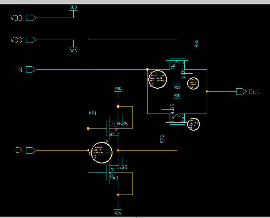
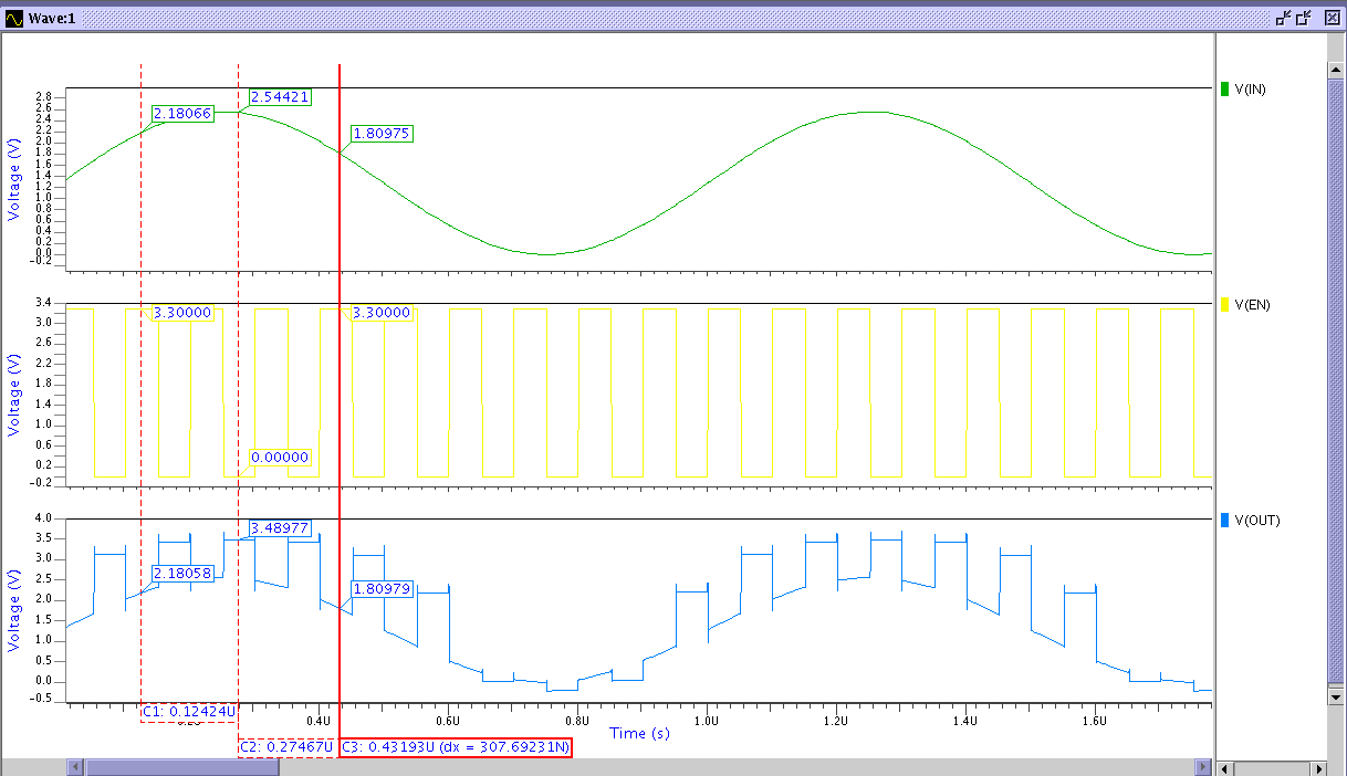
Hi, I would like to know how to determine the size of MOS switches. From what I know, the size should be small in order to have less charge injection but the size should be large to have a small "ON" resistance. Furthermore, I have frequently heard of people making use of half-size dummy switch to reduce charge injection. I would like to know why is it the dummy switch have to be half-size? Another thing that I am not sure of is whether the bulk connection of the NMOS switch should be connected to its source or to the ground. (N-well process) I find that both connection give a different voltage at its terminals. What is the common practice to tie the bulk connection and the reason behind it. Thanks in advance.
 

The on-resistance requirement rather than charge injection determine the minum W. Half size dummu will absobe the injected charge from switch(assume half the charge flow to source and half to drain). Bulk connected to ground.
 

avoid charge injection, you can use cmos switch and two phase clock, which Q1 Q2 and Q2', said Q2' is little more than Q2.
And you can referece some paper or book about adc
 

Dummy switch will have opposite polarity than the switch. You try to keep the falling edge of switch fast. Also dummy switch signal should have some delay compared to normal switch signal so that it can really cancell the charge.
 

Hi, I would like to clarify the statement of "Dummy switch will have opposite polarity than the switch". Do you mean that if the switch is NMOS, then the dummy should be a PMOS? Or do you mean that if the switch is on, then the dummy is off and vice versa? Thanks.
 

hi

when you design a ckt then million of NMOS and PMOS are their. Now if all bulks are connected with gnd/vdd then vth of NMOS/PMOS does not change due to change of bulk voltage becaz all bulks are same potential. Now if you connected with source(when all sources are not connected with gnd) then vth changes due to change of bulk potential....it is effecting in your overall ckt.thanks
 

How should we deal with the bulk voltage of the swtich MOSFETs?
 

Hi,

I am trying to design an analog switch in the technology TSMC 0.35. But I am with some difficulties. My VDD is 3.3V and VSS is 0V.
My design is this:


And the response to the stimulus are this:


What am I doing wrong? Because I want to the V(OUT) goes to 'Z' when the V(EN) is 0V.
I'll use this design in a switched-capacitor A/D.
Thanks
 

Hello, brito.tb!

Your circuit definitely goes to "Z" when V(EN) is 0 V. Voltage of Z-state is indefinitely and meaningless. In your case voltage of Z-state is defined by charge injection from channel of MN2 and MP3 to very small parasitic capacitance at node V(OUT). Try to connect large cap to V(OUT) and you would see that V(OUT) is almost unchangeable when V(EN) goes to 0 V. Or try to connect large res from V(OUT) to VSS and you would see that V(OUT) goes to 0 V.
 

You have a "box" of on resistance vs capacitance that
probably gives you a roughly fixed settling time for a
given process technology. A DC switch and a switched-
capacitor circuit switch want different things and you
might pick one corner of that box over another. Making
gate "on" and "off" voltages track input is a way to
minimize charge injection if you have a lot of headroom
and power to burn. Otherwise your charge injection
will vary with signal common mode position.
 

Thanks to everyone for the help, but I have some questions.
In every book I read, says that is the way to design a switch and never show this "error".
How can I size the transistors to avoid this? And make V(OUT) as close to 0V when V(EN) is 0V?
I need this switch to make this circuit:

Thanks
 

How is your test bench file? If you connect a relatively small resistive load at the output, I don't think the output will be like as what you showed to us.
 

Status
Not open for further replies.

Similar threads

Part and Inventory Search

Welcome to EDABoard.com

Sponsor

Back
Top