Continue to Site

Welcome to EDAboard.com

Welcome to our site! EDAboard.com is an international Electronics Discussion Forum focused on EDA software, circuits, schematics, books, theory, papers, asic, pld, 8051, DSP, Network, RF, Analog Design, PCB, Service Manuals... and a whole lot more! To participate you need to register. Registration is free. Click here to register now.

Design a i/o port that meet -7~12V?

Status
Not open for further replies.

fengluan

Junior Member level 3
Joined
Apr 14, 2006
Messages
27
Helped
0
Reputation
0
Reaction score
0
Trophy points
1,281
Activity points
1,463
90_1190282322.gif


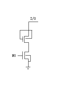
in order to prevent Psub-nwell diode forward conduct when voltage is negetive , a iso-nmos is used. now the problem is whether two nmos may oxide rupture,
the process has BDVds>12V, but Tox is 150A, so Vgs<5V to avoid oxide rupture.

but for my schematic configuration, Vgs(Vgd) some time exceed 5V.
 

There is a doubt how can nmos operate when Vds=12V and BDVgd<5V simultaneously?
U have wrong opinion regarding safe operation regions of MOSs in ur process.
BDVgd can be higher than BDVgs for special device structures. Look in PDK docs or ask FAB about.
 

Status
Not open for further replies.

Part and Inventory Search

Welcome to EDABoard.com

Sponsor

Back
Top