Continue to Site

Welcome to EDAboard.com

Welcome to our site! EDAboard.com is an international Electronics Discussion Forum focused on EDA software, circuits, schematics, books, theory, papers, asic, pld, 8051, DSP, Network, RF, Analog Design, PCB, Service Manuals... and a whole lot more! To participate you need to register. Registration is free. Click here to register now.

Delay locked loop testing

Status
Not open for further replies.

spec07

Junior Member level 2
Joined
Aug 18, 2010
Messages
22
Helped
0
Reputation
0
Reaction score
0
Trophy points
1,281
Activity points
1,414
Hi,

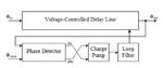
Am I using the correct way if testing the DLL?
1. Set 1 input pulse for clock reference at phase detector input.
2. Set 1 input pulse for clock in with a delay at VCDL input.

Results:
If the DLL is working properly, the clock reference from the phase detector input and clock out from the output of the VCDL would be able to align (lock) after xxx cycles.

Did I get the testing method and the working principle of the DLL correct?

Please advice. Thank you.
 

You can only set clock reference and check the DLL loop regulate the output clk by itself.
 

You can only set clock reference and check the DLL loop regulate the output clk by itself.

What you mean is that I only need 1 external clock pulse which will generate the same clock pulse into the input of the phase detector and the input of VCDL?
 

Yes. Don't input two clocks.
 

a simple DLL has only 1 input which ur clock -- fed to both variable delay line and to phase detector which controls the delay. i dont know how u use reference clock in ur architecture. pls post a schematic/pic of what ur setup and architecture is
 

whats the effect of 2 clocks input? My design is based on the attached. Please advice.
 

Attachments

  • dll.JPG
    dll.JPG
    13.4 KB · Views: 68
Last edited:

if the input to VCDL and PD come from same clock domain (they can the same or a derivative of a clock) then it may not be such a problem else DLL wont work properly.

If the DLL is working properly, the clock reference from the phase detector input and clock out from the output of the VCDL would be able to align (lock) after xxx cycles. -- this alignment may be some constant phase shift as well.

post a shot of input vs output
 

I tried simulating with 1MHz, 10MHz and 100MHz. I got problem with 100MHz, what may be the issue here?
 

100MHz is out of its operating range?
 

100MHz is out of its operating range?

Any ways to make it operate at 100MHz?

---------- Post added at 14:05 ---------- Previous post was at 12:40 ----------

The delay between clk_ref and clk_out is around 12ns and reduces to about 8ns when the output of the charge pump which is vindel saturated. Is there any way which I can reduce the delay even more? This is running at 1MHz. Please see the attached for the simulation results.
 

Attachments

  • DLL_test1MHz.jpg
    DLL_test1MHz.jpg
    308.5 KB · Views: 72
Last edited:

Try to simulate your VCDL cell to find out delay vs controlling voltage to see if u can still reduce delay. i think as long as the delay (8.2ns) remains constant then DLL works fine as your PD can lock to a constant phase value which can result in a constant delay between the input and output
 

Try to simulate your VCDL cell to find out delay vs controlling voltage to see if u can still reduce delay. i think as long as the delay (8.2ns) remains constant then DLL works fine as your PD can lock to a constant phase value which can result in a constant delay between the input and output

I am using 8 delay stages in and a bias circuit in the VCDL, what you mean is that I should reduce the number of delay stages in VCDL in order to reduce the delay of from the start of the simulation to the locking?
 

nope in order to reduce the lock time (start of sim to lock) u need to design the loop filter with more bandwidth, this however is a not always good as it allows more noise and hence more jitter.
 

Yes, you can decrease the delay stage to achieve higher frequency operation.
However, the lower limiter of frequency might be increased too.
I am using 8 delay stages in and a bias circuit in the VCDL, what you mean is that I should reduce the number of delay stages in VCDL in order to reduce the delay of from the start of the simulation to the locking?
 

Yes, you can decrease the delay stage to achieve higher frequency operation.
However, the lower limiter of frequency might be increased too.

Why is decreasing the delay stages able to achieve higher frequency and increase lower limit of frequency? What is the reason behind this? thank you. :)
 

I am not exactly sure about this but i think it is got to do with loop delay, the lower this is the more faster your DLL can respond to it, this i think is causing the frequency range to shift to allow for higher freq operation pushing the lower freq higher
 

Status
Not open for further replies.

Part and Inventory Search

Welcome to EDABoard.com

Sponsor

Back
Top