Continue to Site

Welcome to EDAboard.com

Welcome to our site! EDAboard.com is an international Electronics Discussion Forum focused on EDA software, circuits, schematics, books, theory, papers, asic, pld, 8051, DSP, Network, RF, Analog Design, PCB, Service Manuals... and a whole lot more! To participate you need to register. Registration is free. Click here to register now.

decoupling and power planes connection the right way

Status
Not open for further replies.

Electro nS

Full Member level 6
Joined
Mar 9, 2013
Messages
324
Helped
49
Reputation
98
Reaction score
48
Trophy points
1,308
Activity points
3,818
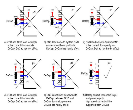
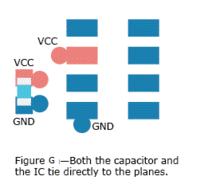
if i am designing a 4 layer board with inner planes Vcc and Gnd
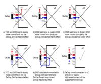
what is the best way to connect the decoupling capacitors to the uC (running at 200Mhz)
i usually use this method :


i have found this on the internet but i am not convensied please give your opinion


High speed decoupling capacitor to be effective should be near to ASIC, Connected with short traces. Planes were connected to CAPACITOR and then capacitor is connected to ASIC. Whatever noise coupled in Plane will be filtered by CAPACITOR will not go to ASIC. ASIC transient current will be coming from Low Impedance source (CAPACITOR) not the POWER PLANE. So, in BOTH ways the last approach is correct.
 
Obviously, the comparison is focussing on injected noise current. But there are other aspects that may be more important in some cases, particularly ground bounce. Also fast analog circuits are often requiring minimal ground inductance and don't allow long fanout traces. Case six clearly fails these requirements.

Other points are that logic chips don't necessarily have equal count of GND and VCC pins, also often use multiple supply voltages. Connecting each ground pin directly to the ground plane, possibly with a microvia inside the pad may be more appropriate in these cases. The bypass capacitors are placed as near to the VCC pins as possible, the exact place of the supply via isn't so important.

If double sided placement is an option, the bypass capacitors may be placed directly under the VCC and GND pins, preferably using plugged vias in pads.

thanks

you have pointed out many important aspects
 

Go for minimum inductance, via's direct to power pins from the planes as above, as the plane capacitance is the second source of power (after the on silicon capacitance), followed by the local decoupling cap (again minimise inductance) then the medium sized reservoir caps and finally the power supply.
Decoupling capacitors provide the instantaneous power requirements, here is some interesting reading...
http://www.hottconsultants.com/techtips/decoupling.html
 

Status
Not open for further replies.

Part and Inventory Search

Welcome to EDABoard.com

Sponsor

Back
Top