Continue to Site
Follow along with the video below to see how to install our site as a web app on your home screen.
Note: This feature may not be available in some browsers.
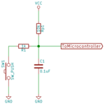
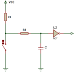
It's easy to do in software.I would like to read the switch in the MCU with a delay of 200 ms to avoid false reading.
Usually I agree with your posts.In post #6 there are two ap notes basically telling us NOT to use
slow rise/fall times of signals into CMOS. Here is another reference -